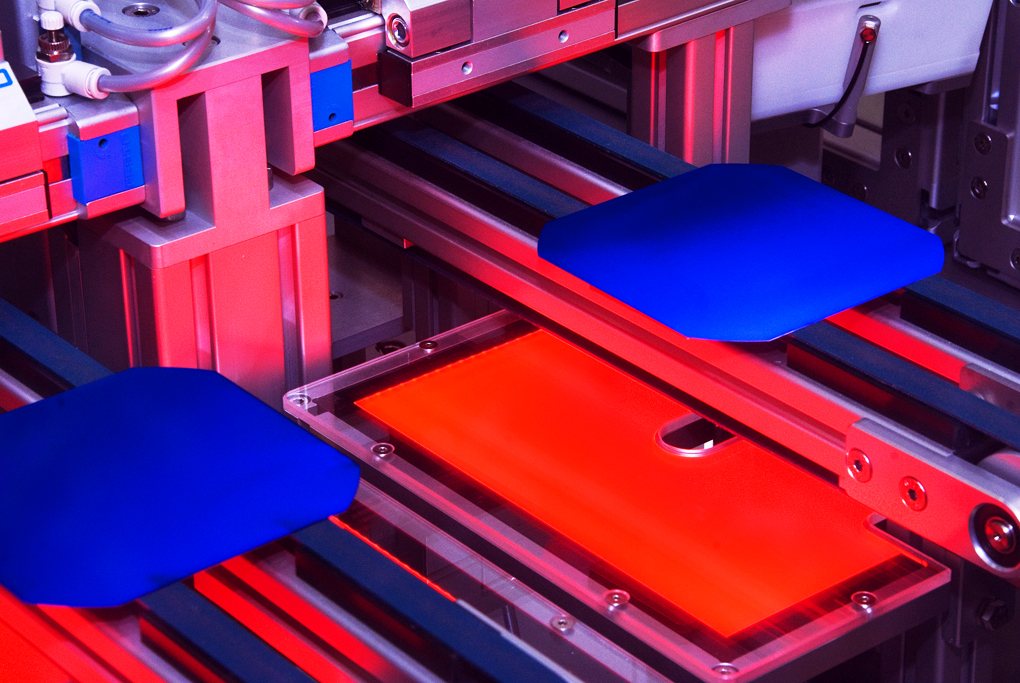
Hold a standard rooftop solar panel and you are holding something that is, by weight, mostly ordinary materials: toughened glass on the front, an aluminium frame around the edge, a plastic backing sheet. Yet the reason it generates electricity at all comes down to a thin layer of treated silicon and a fine web of silver lines you could almost miss. Understanding what each material does — and why substituting it is harder than it looks — is a good way into understanding solar supply chains more broadly.
The silicon core
Silicon is the photovoltaic workhorse. When photons from sunlight strike a silicon crystal, they knock electrons loose, and those electrons can be directed into a circuit. But not any silicon will do. The material must be refined to extremely high purity — ordinary industrial-grade silicon, used in steel and aluminium alloys, contains too many impurities. Solar manufacturers use a grade called polysilicon, which is further processed into either multicrystalline or monocrystalline wafers.
Monocrystalline wafers are cut from a single, carefully grown crystal ingot. Because the atomic lattice is uniform throughout, electrons move through it more efficiently, and monocrystalline panels convert a higher share of sunlight into electricity. Multicrystalline wafers are made by casting molten silicon into blocks and slicing them; the process is cheaper, but grain boundaries in the crystal structure reduce performance somewhat. In recent years, monocrystalline production has grown to dominate the market partly because the efficiency difference matters when roof space or land is limited.
The wafers themselves are extremely thin — imagine a slice not much thicker than a human hair is wide, though a great deal more brittle. Manufacturing them without cracking a significant fraction is one of the less-discussed engineering challenges of solar production.
Silver: the quiet bottleneck
Silver does not generate electricity, but it collects it. On the front face of each cell, a pattern of thin silver lines — called fingers and busbars — forms a grid that gathers the electrons the silicon releases and carries them to the panel's external terminals. Silver is used because it is the best electrical conductor of any element and because it forms reliable contacts with treated silicon surfaces.
The amount of silver per cell is small, but across millions of panels it adds up quickly. To see why this matters, consider an illustrative example. Suppose a panel manufacturer uses a certain number of grams of silver paste per cell and assembles cells into panels at high volume. A modest reduction in silver per cell — achieved through finer printing or by replacing some busbars with copper — translates into a large absolute saving across an entire production run. This is why the solar industry has been steadily reducing silver consumption per watt of capacity over many years, not because silver stops working, but because the metal is expensive and its mining is tied to primary production of lead, zinc and copper rather than being mined in large quantities for its own sake.
The solar sector now competes with electronics, jewellery and industrial uses for available silver, which makes the industry's relationship with the metal a genuine supply-chain question rather than a minor detail.
Glass and aluminium: structure and protection
The front sheet of a standard panel is tempered, low-iron glass. Ordinary glass has a greenish tint caused by iron content, which absorbs some light before it reaches the silicon. Low-iron glass is more transparent and allows more photons through. The tempering process makes the sheet far more resistant to hail, wind load and thermal stress than ordinary window glass.
The aluminium frame holds the laminated assembly rigid, allows it to be mounted on a roof or ground structure, and provides a grounding point for electrical safety. It is not a particularly exotic application of aluminium, but the volume is substantial when multiplied across global panel production, and the alloy specification matters because the frame must resist corrosion over a design life measured in decades.
Between the glass and the silicon cells, and between the cells and the back sheet, thin layers of encapsulant — typically a polymer called EVA, ethylene vinyl acetate — hold everything together and exclude moisture. The back sheet is usually a white or transparent polymer film. Neither material is rare, but the long-term durability of the encapsulant under ultraviolet exposure is a subject of ongoing materials research.
Thin-film alternatives
Silicon panels dominate the market, but they are not the only approach. Thin-film solar cells deposit light-absorbing semiconductor material directly onto glass or flexible substrates in layers far thinner than a silicon wafer. The three main commercial thin-film technologies use different absorber materials: cadmium telluride (CdTe), copper indium gallium selenide (CIGS), and amorphous silicon.
Cadmium telluride panels have become the most commercially significant thin-film product. They use far less semiconductor material than crystalline silicon panels, but they introduce different supply considerations: tellurium is a byproduct of copper refining and is produced in comparatively small quantities globally, and cadmium is a toxic heavy metal that requires careful handling and end-of-life management.
CIGS panels absorb sunlight across a broader part of the spectrum than CdTe and can reach high efficiencies in laboratory conditions, but manufacturing them consistently at scale has proved more difficult. They depend on indium, which is also a byproduct metal — primarily from zinc refining — and gallium, which comes mainly from aluminium production. Neither is abundant in the way silicon is.
Amorphous silicon thin-film panels use the same base element as conventional panels but deposit it in a disordered, non-crystalline form. This requires less material and can be applied to flexible surfaces, but conversion efficiency is lower than crystalline silicon.
Putting it together: an illustrative comparison
Suppose, for illustration, that you are comparing two panels with the same power output. A crystalline silicon panel achieves that output in a smaller area because of higher efficiency, but it requires processed polysilicon and a measurable quantity of silver. A CdTe thin-film panel covering more area to achieve the same output avoids silicon and silver but requires tellurium and cadmium. Neither is simply better from a materials perspective; they represent different trade-offs between efficiency, material scarcity and manufacturing complexity.
Where to go next
Readers with a closer interest in the industry will find that the story gets more detailed quickly. The shift from aluminium back-surface-field cells to passivated emitter and rear contact (PERC) and tunnel oxide passivated contact (TOPCon) architectures changes silver consumption patterns significantly. Perovskite solar cells — which can be layered on top of silicon in tandem configurations — introduce a further set of materials questions around lead content and long-term stability that are the subject of active research.