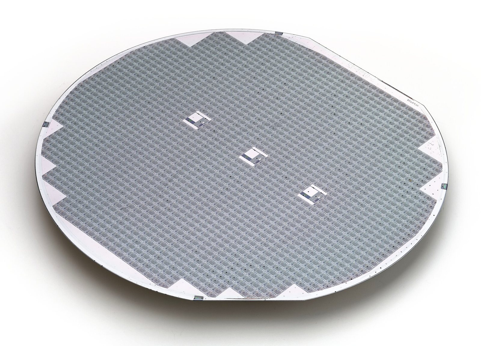
Lo que es
Material quantities per chip are tiny; the binding constraints are purity and the number of qualified suppliers, not tonnage. A single contaminated gas shipment can idle a fab.
La lista de materiales
Escálelo →Las cantidades son per 300 mm waferrango indicativo
| Material | Bajo | Alto | Unidad | Base |
|---|---|---|---|---|
| Silicon crítico | 0.12 | 0.15 | kg | One 300 mm wafer weighs about 125 g |
| Hafnium crítico Milligrams per wafer, with no substitute. | traza | traza | kg | Atomic-layer gate dielectric |
| Helium Consumed as gas, not incorporated. | traza | traza | kg | Process cooling and leak detection |
| High-Purity Quartz Consumption is per ingot, not per wafer. | traza | traza | kg | Consumed as crucible during crystal growth |
| Tungsten crítico Grams per wafer. | traza | traza | kg | Contacts and vias |
Indicative range compiled from published technology studies and chemistry; verify against a manufacturer specification before use. Las filas marcadas como «traza» contienen el material en cantidades demasiado pequeñas para expresarse de forma útil como masa; la restricción allí es la pureza o el número de proveedores, no el tonelaje.
Las alternativas
La sustitución es la fuerza más subestimada en materiales. Cuando un metal se encarece o resulta políticamente problemático, los ingenieros diseñan soluciones alternativas — y la demanda de una mina entera puede desvanecerse.

Cadmium Telluride Thin-Film Module
A solar panel a few microns thick, using no silicon at all.
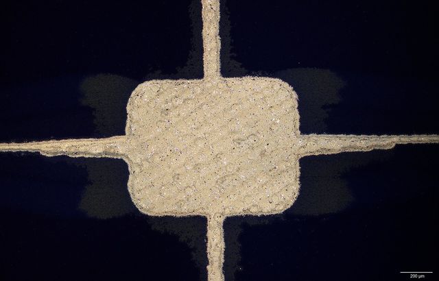
Crystalline Silicon Solar Module
The standard solar panel: silicon wafers, silver contact paste, glass and an aluminium frame.
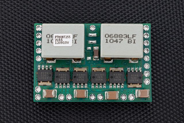
Gallium Nitride Power Device
A switch that turns on and off far faster than silicon, so power supplies can shrink.