Commercial
Semiconductors
それが何であるか
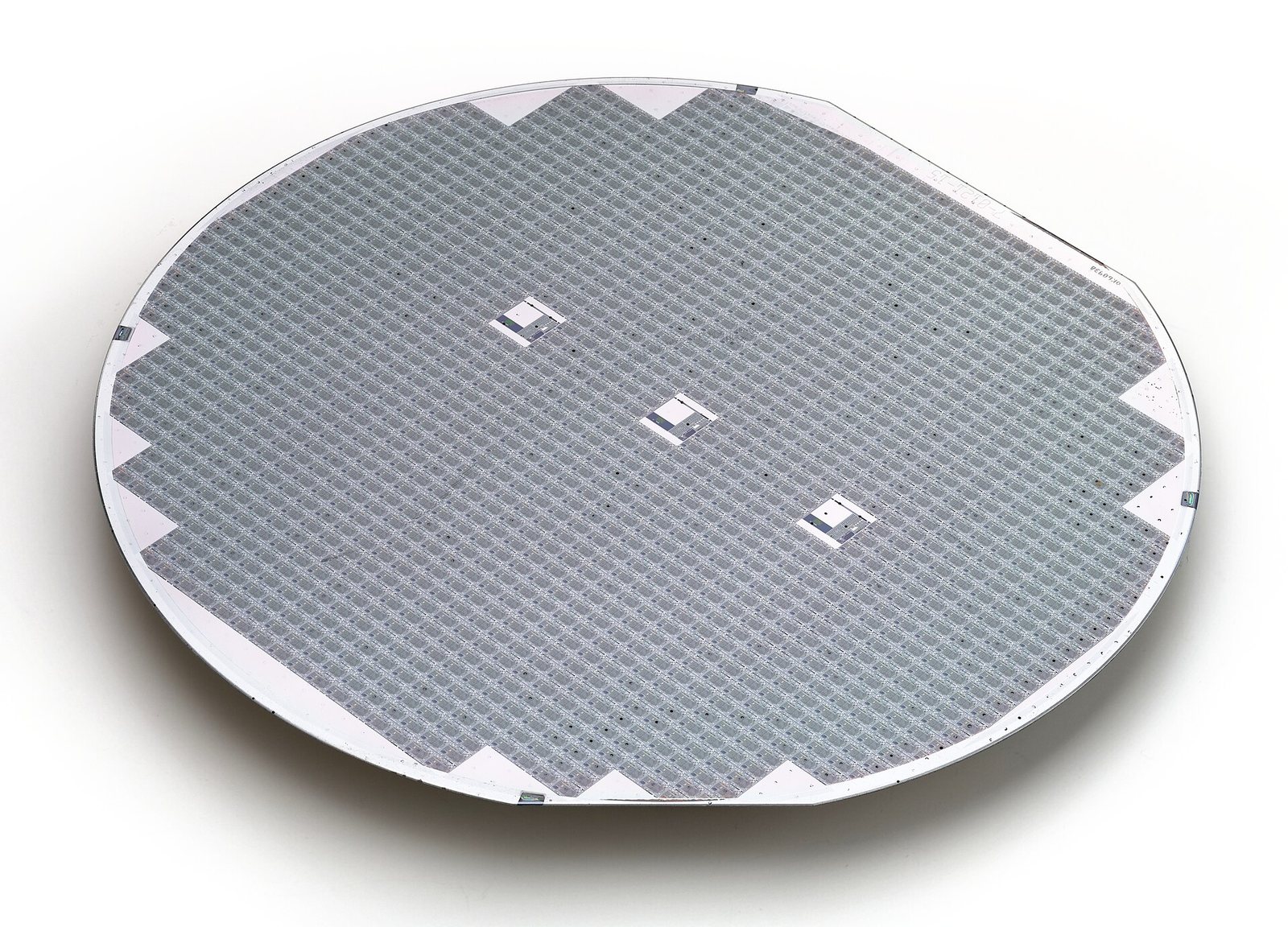
Material quantities per chip are tiny; the binding constraints are purity and the number of qualified suppliers, not tonnage. A single contaminated gas shipment can idle a fab.
素材の明細
スケールアップ →数量の単位 per 300 mm wafer参考レンジ
「おおよそこの程度、多少の幅あり」として読んでください。メーカーごとに設計は異なり、エンジニアが高価な素材の使用量を削減するにつれ、数値は時間とともに低下します。
| 素材 | 低 | 高 | 単位 | 基準 |
|---|---|---|---|---|
| Silicon クリティカル | 0.12 | 0.15 | kg | One 300 mm wafer weighs about 125 g |
| Hafnium クリティカル Milligrams per wafer, with no substitute. | 微量 | 微量 | kg | Atomic-layer gate dielectric |
| Helium Consumed as gas, not incorporated. | 微量 | 微量 | kg | Process cooling and leak detection |
| High-Purity Quartz Consumption is per ingot, not per wafer. | 微量 | 微量 | kg | Consumed as crucible during crystal growth |
| Tungsten クリティカル Grams per wafer. | 微量 | 微量 | kg | Contacts and vias |
Indicative range compiled from published technology studies and chemistry; verify against a manufacturer specification before use. 「微量(trace)」と表示された行は、質量として有意に示せないほど微量の素材を含む行です。制約となるのはトン数ではなく、純度またはサプライヤー数です。
代替手段
代替は材料分野で最も過小評価されている力である。金属が高騰したり調達が政治的に困難になったりすると、エンジニアはそれを使わない設計を考案し、鉱山一つ分の需要が丸ごと消滅することもある。

Cadmium Telluride Thin-Film Module
A solar panel a few microns thick, using no silicon at all.
Crystalline Silicon Solar Module
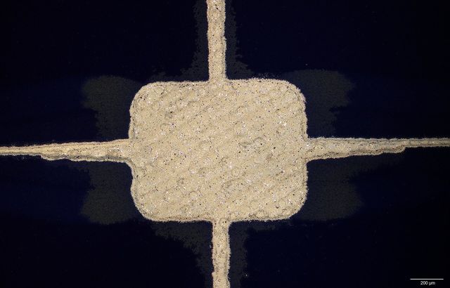
The standard solar panel: silicon wafers, silver contact paste, glass and an aluminium frame.
Gallium Nitride Power Device
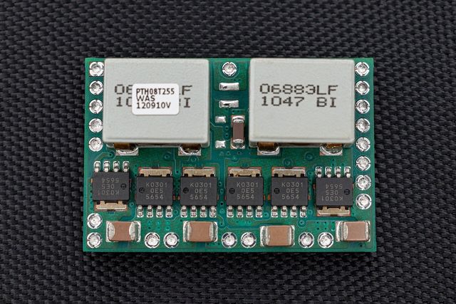
A switch that turns on and off far faster than silicon, so power supplies can shrink.