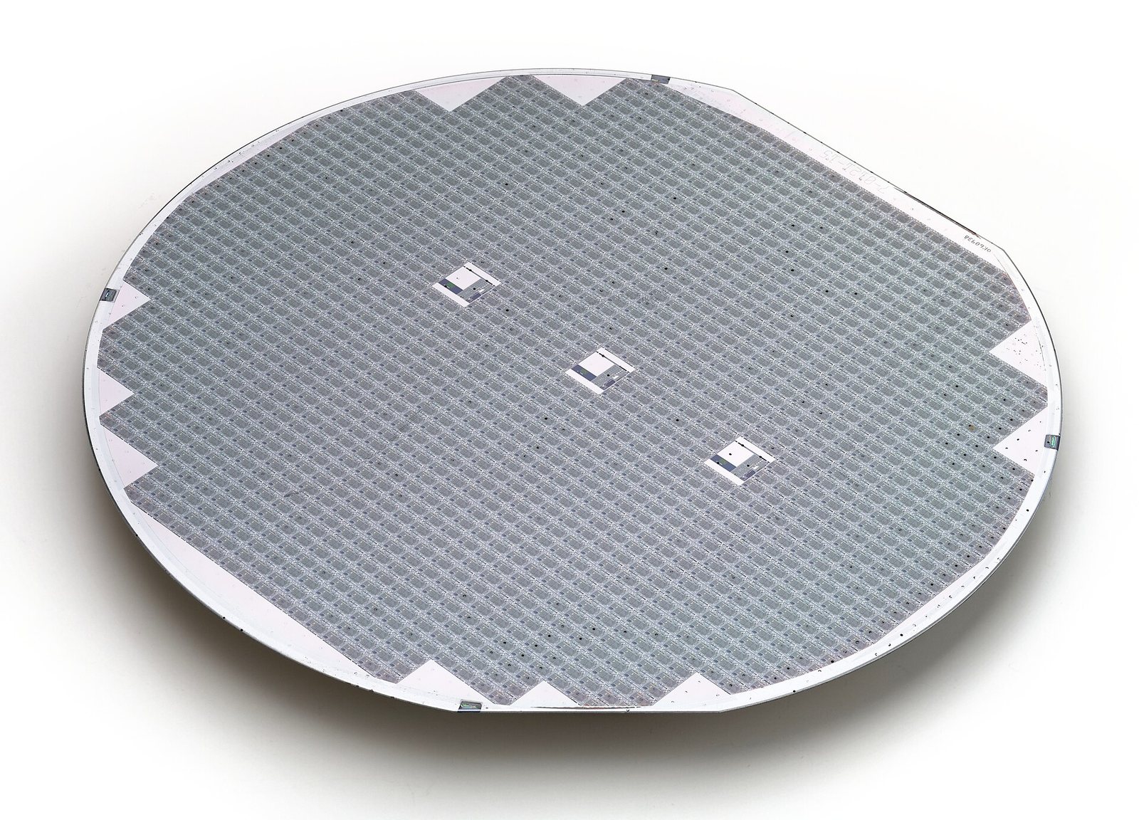
정의
Material quantities per chip are tiny; the binding constraints are purity and the number of qualified suppliers, not tonnage. A single contaminated gas shipment can idle a fab.
소재 명세
규모 확대 →수량 단위 per 300 mm wafer참고 범위
| 소재 | 낮음 | 높음 | 단위 | 기준 |
|---|---|---|---|---|
| Silicon 핵심 광물 | 0.12 | 0.15 | kg | One 300 mm wafer weighs about 125 g |
| Hafnium 핵심 광물 Milligrams per wafer, with no substitute. | 미량 | 미량 | kg | Atomic-layer gate dielectric |
| Helium Consumed as gas, not incorporated. | 미량 | 미량 | kg | Process cooling and leak detection |
| High-Purity Quartz Consumption is per ingot, not per wafer. | 미량 | 미량 | kg | Consumed as crucible during crystal growth |
| Tungsten 핵심 광물 Grams per wafer. | 미량 | 미량 | kg | Contacts and vias |
Indicative range compiled from published technology studies and chemistry; verify against a manufacturer specification before use. "미량(trace)"으로 표시된 행은 질량으로 유의미하게 나타내기에 너무 적은 양이 포함된 것입니다. 이 경우 제약 요인은 순도 또는 공급업체 수이며, 톤수가 아닙니다.
대안
대체는 소재 분야에서 가장 과소평가된 힘이다. 금속이 비싸지거나 정치적으로 조달이 어려워지면, 엔지니어들은 그것을 우회하는 설계를 택하고 — 광산 하나의 수요 전체가 소멸할 수 있다.

Cadmium Telluride Thin-Film Module
A solar panel a few microns thick, using no silicon at all.
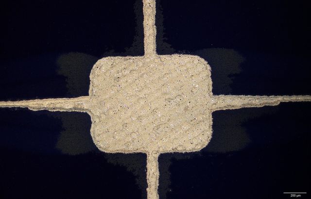
Crystalline Silicon Solar Module
The standard solar panel: silicon wafers, silver contact paste, glass and an aluminium frame.
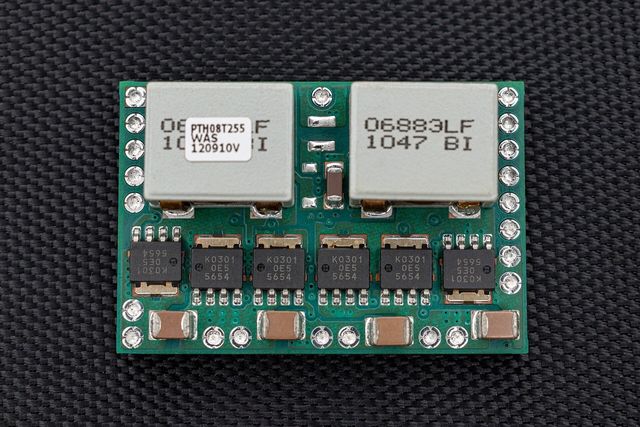
Gallium Nitride Power Device
A switch that turns on and off far faster than silicon, so power supplies can shrink.