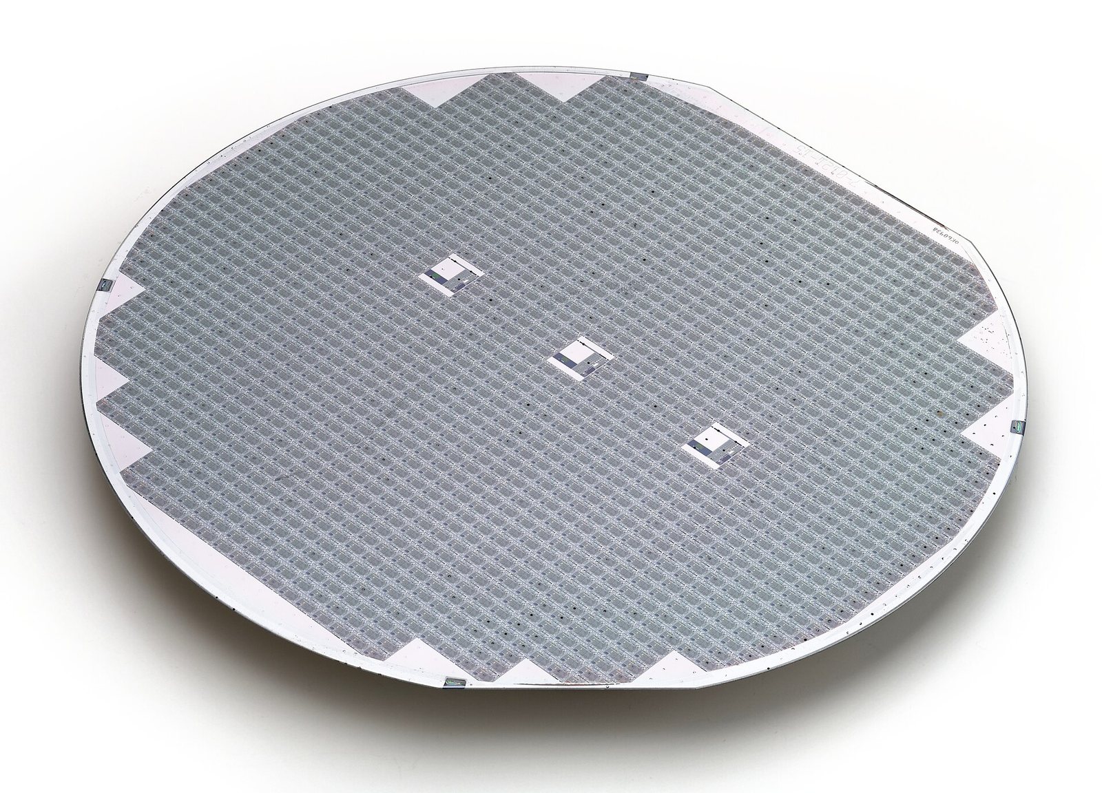
Nedir
Material quantities per chip are tiny; the binding constraints are purity and the number of qualified suppliers, not tonnage. A single contaminated gas shipment can idle a fab.
Malzeme listesi
Ölçeği büyütün →Miktarlar per 300 mm wafergösterge aralığı
| Materyal | Düşük | Yüksek | Birim | Dayanak |
|---|---|---|---|---|
| Silicon kritik | 0.12 | 0.15 | kg | One 300 mm wafer weighs about 125 g |
| Hafnium kritik Milligrams per wafer, with no substitute. | iz | iz | kg | Atomic-layer gate dielectric |
| Helium Consumed as gas, not incorporated. | iz | iz | kg | Process cooling and leak detection |
| High-Purity Quartz Consumption is per ingot, not per wafer. | iz | iz | kg | Consumed as crucible during crystal growth |
| Tungsten kritik Grams per wafer. | iz | iz | kg | Contacts and vias |
Indicative range compiled from published technology studies and chemistry; verify against a manufacturer specification before use. "İz" olarak işaretlenmiş satırlar, ilgili malzemeyi kütle olarak anlamlı biçimde ifade edilemeyecek kadar küçük miktarlarda içerir — buradaki kısıt tonnaj değil, saflık veya tedarikçi sayısıdır.
Alternatifler
İkame, malzeme biliminde en az takdir edilen güçtür. Bir metal pahalı ya da siyasi açıdan güç hale geldiğinde, mühendisler onu devre dışı bırakacak tasarımlar yapar — ve tüm bir madenin talebi buharlaşabilir.

Cadmium Telluride Thin-Film Module
A solar panel a few microns thick, using no silicon at all.
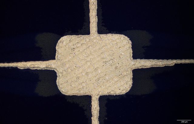
Crystalline Silicon Solar Module
The standard solar panel: silicon wafers, silver contact paste, glass and an aluminium frame.
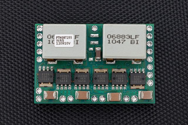
Gallium Nitride Power Device
A switch that turns on and off far faster than silicon, so power supplies can shrink.