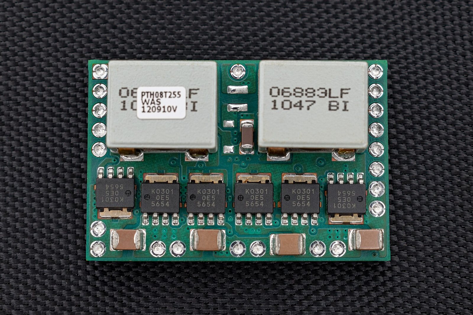
यह क्या है
GaN is why a laptop charger the size of a matchbox exists. It also cuts conversion losses in data centres and solar inverters, which matters at gigawatt scale.
सामग्री विवरण
इसे बड़े पैमाने पर करें →मात्राएँ हैं per deviceसांकेतिक परास
| सामग्री | निम्न | उच्च | इकाई | आधार |
|---|---|---|---|---|
| Gallium क्रिटिकल Grams; the constraint is refining capacity, not tonnage. | अनुरेख | अनुरेख | kg | Substrate and epitaxial layer |
| Silicon क्रिटिकल | अनुरेख | अनुरेख | kg | Common substrate for GaN-on-Si |
Indicative range compiled from published technology studies and chemistry; verify against a manufacturer specification before use. "ट्रेस" चिह्नित पंक्तियों में वह सामग्री इतनी कम मात्रा में होती है कि उसे द्रव्यमान के रूप में उपयोगी रूप से व्यक्त नहीं किया जा सकता — वहाँ सीमा टनभार की नहीं, शुद्धता या आपूर्तिकर्ता संख्या की है।
विकल्प
प्रतिस्थापन सामग्रियों में सबसे कम आँकी गई शक्ति है। जब कोई धातु महँगी या राजनीतिक दृष्टि से कठिन हो जाती है, तो इंजीनियर उसे दरकिनार कर डिज़ाइन करते हैं — और पूरी एक खान की माँग वाष्पित हो सकती है।
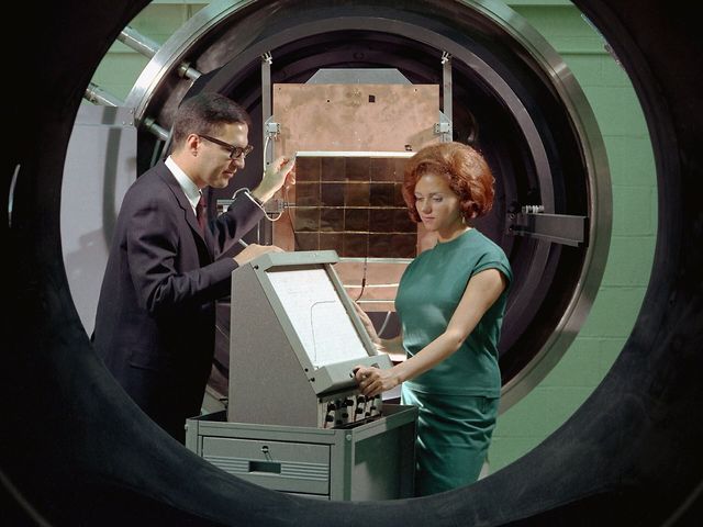
Cadmium Telluride Thin-Film Module
A solar panel a few microns thick, using no silicon at all.
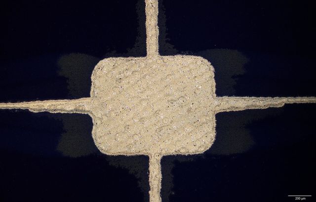
Crystalline Silicon Solar Module
The standard solar panel: silicon wafers, silver contact paste, glass and an aluminium frame.
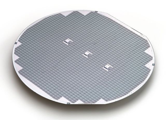
Leading-Edge Logic Chip
The most advanced processors, built on wafers that pass through hundreds of process steps.