Scaling
Data Centres & AI
其定义
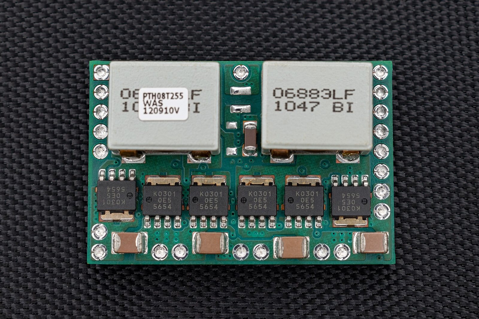
GaN is why a laptop charger the size of a matchbox exists. It also cuts conversion losses in data centres and solar inverters, which matters at gigawatt scale.
材料清单
放大规模 →数量为 per device参考区间
将这些数据理解为"大致如此,存在一定误差"。每家制造商的设计各有不同,且随着工程师逐步减少对高价物料的用量,数据会随时间下降。
| 材料 | 低 | 高 | 单位 | 基准 |
|---|---|---|---|---|
| Gallium 关键 Grams; the constraint is refining capacity, not tonnage. | 痕量 | 痕量 | kg | Substrate and epitaxial layer |
| Silicon 关键 | 痕量 | 痕量 | kg | Common substrate for GaN-on-Si |
Indicative range compiled from published technology studies and chemistry; verify against a manufacturer specification before use. 标注为"微量"的行表示该物料含量极低,无法以质量形式有效表达——其制约因素在于纯度或供应商数量,而非吨位。
替代方案
替代是材料领域最被低估的力量。当某种金属价格高涨或在政治上难以获取时,工程师便会绕开它进行设计——整座矿山的需求可能因此消失殆尽。

Cadmium Telluride Thin-Film Module
A solar panel a few microns thick, using no silicon at all.
Crystalline Silicon Solar Module
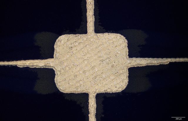
The standard solar panel: silicon wafers, silver contact paste, glass and an aluminium frame.
Leading-Edge Logic Chip
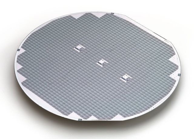
The most advanced processors, built on wafers that pass through hundreds of process steps.