素材にとっての重要性
Modern logic uses about two-thirds of the stable elements somewhere in its process flow. Purity, not tonnage, is the constraint: parts per billion matter, and only a handful of suppliers on Earth can hold that specification.
その組成
全素材 →| 素材 | ここでの機能 | 重要度 |
|---|---|---|
| Copper クリティカル | On-chip interconnect | 定義 |
| Gallium クリティカル | Compound semiconductors for RF and power | 定義 |
| Hafnium クリティカル | High-k transistor gate dielectric | 定義 |
| High-Purity Quartz | Crucibles for crystal growth | 定義 |
| Silicon クリティカル | The wafer | 定義 |
| Tungsten クリティカル | Contacts and vias | 定義 |
| Arsenic クリティカル | Dopant and GaAs | 重要 |
| Cobalt クリティカル | Liner and interconnect at small nodes | 重要 |
| Germanium クリティカル | SiGe transistors and optics | 重要 |
| Gold | Bonding and plating | 重要 |
| Helium | Cooling and leak detection | 重要 |
| Indium クリティカル | Transparent contacts and III-V devices | 重要 |
| Ruthenium クリティカル | Interconnect at the smallest nodes | 重要 |
| Silicon Carbide & Abrasives | Silicon carbide power devices and wafer polishing | 重要 |
| Tantalum クリティカル | Diffusion barrier and capacitors | 重要 |
| Tin クリティカル | EUV light source and solder | 重要 |
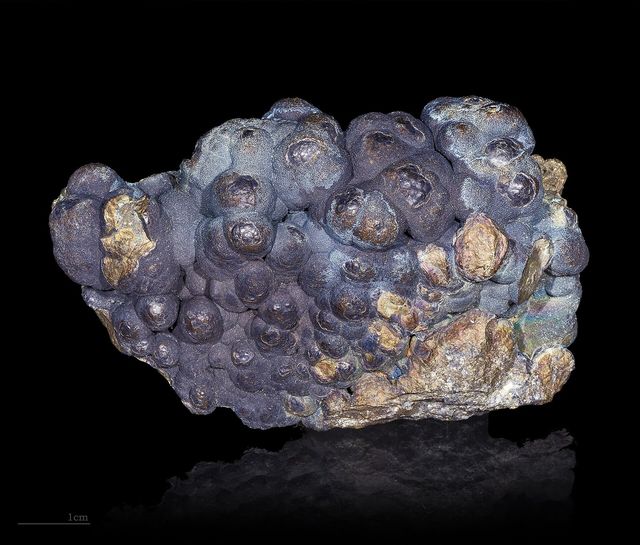
Copper
The reddish metal that carries electricity better than anything except silver, and which humans have been smelting…
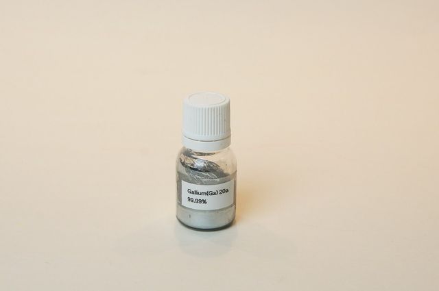
Gallium
A silvery metal that melts in your hand, and the basis of the compound semiconductors in fast chargers, radar and…
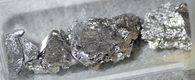
Hafnium
Zirconium's chemical shadow — always found with it, almost impossible to separate from it, and the opposite of it in…
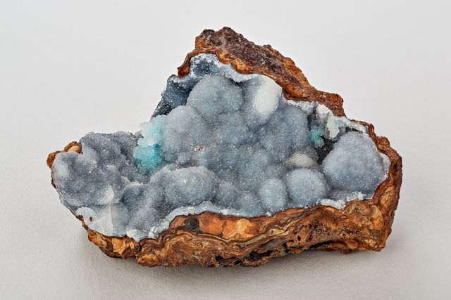
High-Purity Quartz
Quartz sand so free of other elements that it can be melted into the crucible a silicon crystal is grown inside.
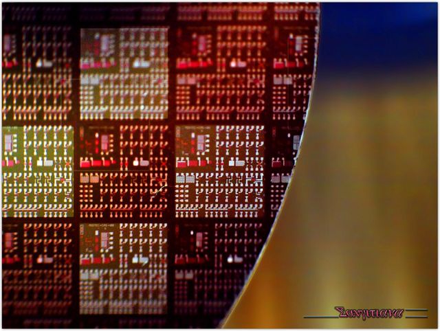
Silicon
The second-most-common element in the Earth's crust — ordinary sand — purified until only one atom in a billion is…
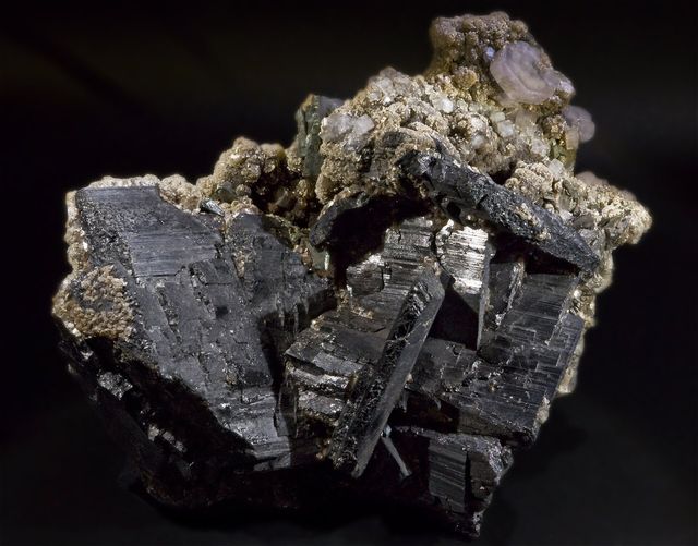
Tungsten
The metal with the highest melting point of them all — you can heat it to 3,400 C before it turns liquid.