鉱石から製品まで、経路を追跡
The Materials Atlas
素材 鉱山・鉱床 処理・精製 管理移転経路 サプライチェーン 企業 ニュース
棚別素材 バッテリー材料 希土類元素 銅・電気 半導体材料 核物質 航空宇宙・防衛 貴金属 鉄鋼・合金金属 工業用鉱物 農業用鉱物 エネルギー原材料 鉱石鉱物 周期表
需要 最終市場 技術 素材計算機 地図 スクリーナー
学習・ツール 学ぶ用語集 データに質問するAIエージェント 調査・データAPI ★ 保存済み
概要 運営について方法論 データソースお問い合わせ 免責事項
表示オプション
🧭 ガイドビュー 鉱石品位、精鉱、精錬、副産物といった用語が初めての方へ。閲覧しながらすべての用語をわかりやすく解説します。同じデータを、解説付きでご覧いただけます。
⚡ 専門家向け解説 業界の知識はお持ちのはず。データのみを——簡潔、迅速、コンパクトに、余分な説明なしで。これがデフォルト表示です。
テーマ
インターフェース言語
深度 素材ページは4段階のレベルで構成されている。任意の素材ページでレベルを選択すると、その設定が記憶される。
★ 保存済み 調査・データ
Silicon

半導体材料

Silicon Si · 14

The second-most-common element in the Earth's crust — ordinary sand — purified until only one atom in a billion is something else.

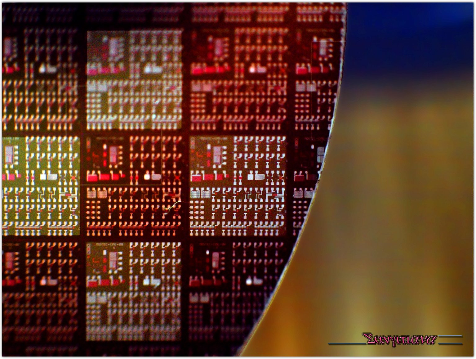
Wafer 20110212 · Sangitiana Fararano · CC BY-SA 2.0 · Wikimedia Commons

これは何か

The second-most-common element in the Earth's crust — ordinary sand — purified until only one atom in a billion is something else.

なぜ重要なのか

Every chip and almost every solar panel starts as a single silicon crystal. The purification, not the raw material, is the hard part.

Where it is in the Earth

Silicon is the second most abundant element in the Earth's crust, yet it almost never occurs in pure metallic form. In nature it bonds immediately with oxygen, forming silicon dioxide (quartz) and a broad family of silicate minerals that make up the bulk of common rocks — granite, sandstone, quartzite, and many others. The sheer prevalence of silicon-bearing rock is not, on its own, what makes a deposit worth mining. What matters is finding quartz that is both physically concentrated and chemically clean enough to feed a smelter without excessive pre-treatment.

The most useful deposits are high-purity quartzite — metamorphic rock in which ancient sandy sediments were compressed and recrystallised by heat and pressure deep in the crust over hundreds of millions of years. That metamorphic process can flush out many impurities, leaving behind masses of nearly pure silicon dioxide. Major deposits of this kind are found in Norway, Brazil, and parts of North America and Australia. A separate and more abundant source is unconsolidated silica sand, formed when quartz-rich rocks weather and the grains accumulate in river beds, beaches, and dunes. Sand is cheaper to extract but typically carries more iron, aluminium, and other contaminants that must be removed before the material can be smelted into silicon metal.

The geography of silicon production therefore reflects two separate things: where clean quartz happens to be concentrated by geology, and where cheap electricity is available to run the energy-intensive smelting furnaces. A country can have excellent quartzite and still not smelt much silicon if power costs are high, or it can import ore and smelt it locally if electricity is cheap. Norway and Iceland, for instance, exploit abundant hydroelectric power. China's dominance reflects a combination of domestic quartz resources, coal-powered electricity, and decades of deliberate industrial scaling.

Getting it out

Silicon metal starts life as mined quartz or quartzite, and in almost every case the mine is an open pit. The rock sits at or near the surface in large, coherent masses, which makes underground working unnecessary and uneconomic. Quartzite is blasted with explosives, loaded onto haul trucks, and crushed at a primary crushing plant near the pit. Because quartz is the target mineral rather than a trace metal dispersed through host rock, the ore grades are high — the material mined is predominantly the useful mineral itself. There is relatively little of what miners call waste rock, the barren material that must be moved but contains nothing saleable.

The practical challenge is not extracting enough silicon dioxide but extracting it at sufficient purity. Even a quartzite body that looks uniform to the eye will contain veins and pockets of feldspar, mica, iron oxides, and other minerals. Mining therefore involves selective extraction — working those parts of the deposit that assay below certain thresholds for iron, aluminium, calcium, and other elements that would degrade the final metal. Ore that fails purity tests may be stockpiled separately or sold to lower-grade markets such as the construction aggregate or glass industries. This selectivity means the effective yield from a given volume of rock is lower than the raw abundance of quartz would suggest.

Silica sand operations follow a different pattern. The unconsolidated sand is dredged or scraped from the surface with minimal blasting, then washed and classified by particle size. Because the starting purity is lower than quartzite, sand operations typically invest more heavily in wet processing — scrubbing, magnetic separation, and flotation — before the material leaves the mine site. The result is a product still well short of silicon metal purity, requiring smelting to go further.

What pulls on it

Silicon has two largely separate demand streams that happen to start from the same element. The first is metallurgical: steel and aluminium producers use ferrosilicon and silicon metal as alloying agents to harden metals and remove dissolved oxygen, and the chemical industry uses silicon metal as the feedstock for silicone polymers and silicon tetrachloride. These markets are large, mature, and tied broadly to construction activity, automotive production, and industrial output. They do not require ultra-high purity and they absorb the bulk of the silicon produced globally by volume.

The second stream is the electronics and energy transition market, which demands polysilicon and, ultimately, single-crystal wafers. Solar photovoltaic manufacturing has become the dominant growth driver here. A crystalline silicon solar module requires between 2,500 and 4,000 kg of polysilicon per megawatt of generating capacity — a substantial physical quantity that scales directly with the rate of solar installation. Semiconductor demand, by contrast, uses far smaller quantities of silicon by weight (a single 300 mm wafer weighs roughly 125 grams, and the silicon content of finished chips is a small fraction of that), but the value embedded in each kilogram is vastly higher and the purity requirements are far more exacting.

For silicon demand to shift sharply downward in electronics, chip architectures would need to migrate away from silicon substrates entirely — something the industry has pursued incrementally with materials such as gallium nitride and silicon carbide for specific power applications, but not at a scale that threatens silicon's overall volume. In solar, a move away from crystalline silicon toward thin-film alternatives would reduce polysilicon demand, but crystalline silicon retains strong efficiency and cost advantages that have kept its market share dominant. The clearer upward pressure on demand comes from continued solar deployment, electric vehicle power electronics, and data-centre expansion, all of which draw on different parts of the silicon supply chain simultaneously.

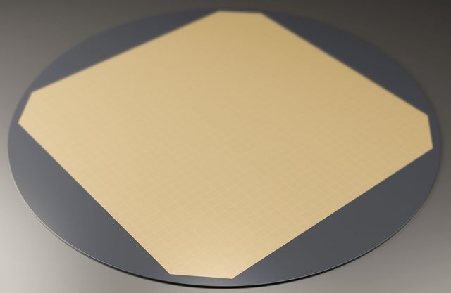
数値の読み方に注意してください。 USGS silicon figures are silicon CONTENT of ferrosilicon plus silicon metal, not polysilicon. Metallurgical-grade silicon (~99%), then polysilicon (99.9999999%), then a grown ingot, then wafers.

岩石中の産出箇所

全鉱石鉱物 →

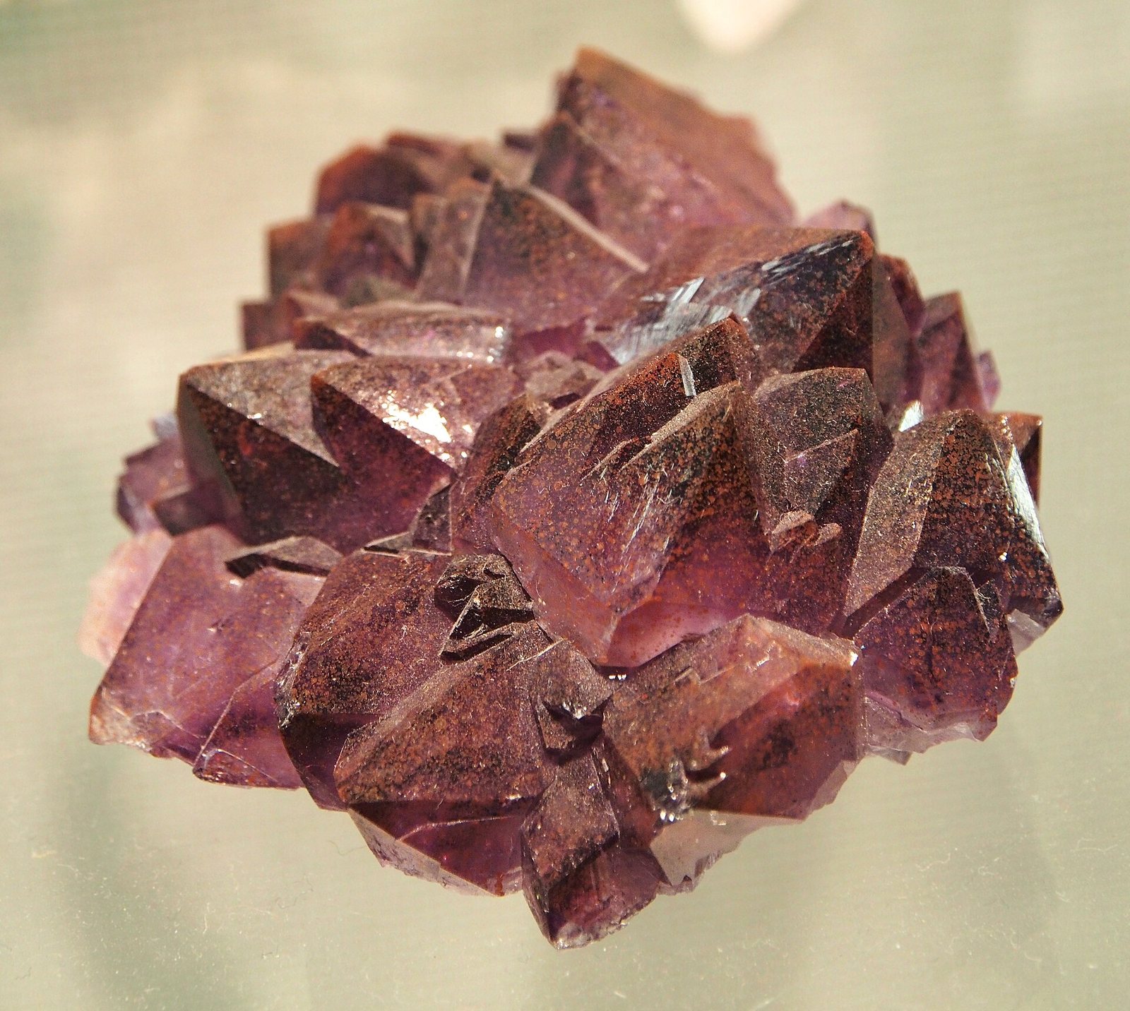
実際に以下を担う鉱物 silicon. 鉱床が鉱体となるのは、採掘コストを回収できるほど十分な濃度で鉱石が濃集している場合に限られる。
この素材については複数のシリーズが発行されている。 USGSがこれらを別々に報告しているのは、鉱山産出量と精製所産出量、または異なる化学的基準など、異なる事象を測定しているためです。別々の表として表示しており、合算してはなりません。

Ferrosilicon

Ferrosiliconthousand metric tons 2025 (推定値) 世界合計 5,000 thousand metric tons

USGS Mineral Commodity Summaries 2026 · USGS silicon figures are silicon CONTENT of ferrosilicon plus silicon metal, not polysilicon. · 出典 ↗

テーブルを横にスクロールすると残りの列が表示されます。

生産 世界に占める割合
China 3,500 70.0%
Russia 420.0 8.4%
Brazil 170.0 3.4%
Norway 150.0 3.0%
Other countries 140.0 2.8%
Kazakhstan 120.0 2.4%
Malaysia 120.0 2.4%
Bhutan 98.00 2.0%
Iceland 72.00 1.4%
India 59.00 1.2%
Spain 40.00 0.8%
South Africa 35.00 0.7%
Canada 23.00 0.5%
France 21.00 0.4%
United States Withheld
Australia Zero
Germany Zero
世界合計 5,000100%

Silicon metal

Silicon metalthousand metric tons 2025 (推定値) 世界合計 4,600 thousand metric tons

USGS Mineral Commodity Summaries 2026 · USGS silicon figures are silicon CONTENT of ferrosilicon plus silicon metal, not polysilicon. · 出典 ↗

テーブルを横にスクロールすると残りの列が表示されます。

生産 世界に占める割合
China 4,000 87.0%
Brazil 180.0 3.9%
Norway 130.0 2.8%
France 68.00 1.5%
Australia 47.00 1.0%
Other countries 46.00 1.0%
Russia 35.00 0.8%
Canada 34.00 0.7%
Iceland 16.00 0.3%
Germany 13.00 0.3%
South Africa 10.00 0.2%
Kazakhstan 7.00 0.2%
Spain 4.00 0.1%
India Zero
Malaysia Zero
United States Withheld
Bhutan Zero
世界合計 4,600100%

「非開示」とは、個別企業のデータが特定されないようUSGSが数値を公表しなかったことを意味し、ゼロを意味するものではありません。出典が各数値を独立して丸め処理しており、「その他の国」の内訳を常に示しているわけではないため、各国の数値の合計が世界合計と一致しないことがあります。

価格

average, cents per pound of silicon: Silicon metal

年間平均cents per pound

2021 · 220.3 高 361.9 cents per pound 2025 · 130.0

基準: average, cents per pound of silicon: Silicon metal. 以下に公表された年間平均値: USGS Mineral Commodity Summaries 2026 · 出典 ↗. これらは参照用の年間平均値であり、リアルタイムの市況相場ではない。

average, cents per pound of silicon: Ferrosilicon, 75% silicon

年間平均cents per pound

2021 · 192.3 高 312.1 cents per pound 2025 · 140.0

基準: average, cents per pound of silicon: Ferrosilicon, 75% silicon. 以下に公表された年間平均値: USGS Mineral Commodity Summaries 2026 · 出典 ↗. これらは参照用の年間平均値であり、リアルタイムの市況相場ではない。

処理・精製が行われる場所

プラント種別 ステージ役割
Samsung Pyeongtaek Campus 半導体製造工場コンポーネント South Korea投入
TSMC Fab 18, Tainan 半導体製造工場コンポーネント Taiwan投入
Hemlock Semiconductor Polysilicon Plant 化学プラント精製 United States投入
Xinjiang & Inner Mongolia Polysilicon Cluster 化学プラント精製 China投入
最終市場そこでの機能重要度
Data Centres & AI Processors, memory and power conversion 定義
Solar Power The cell itself 定義
Semiconductors The wafer 定義
Consumer Electronics Every chip 定義
Robotics & Automation Controllers and sensors 定義
Electric Vehicles Power electronics and anode additive 重要
Power Grids Grid-scale power electronics and HVDC valves 重要

技術が必要とする量

「インテンシティ」とは、ある製品1単位に含まれる素材の量を指します。ここに示す値は参考レンジであり、実際の設計はメーカーやモデル年によって異なります。また、エンジニアが使用量を削減する技術を習得するにつれ、いずれの値も低下し続けています。
技術数量 建値基準
Crystalline Silicon Solar Module 2,500–4,000 kg per MW of capacityPolysilicon in the wafers
Gallium Nitride Power Device 微量 per deviceCommon substrate for GaN-on-Si
Leading-Edge Logic Chip 0.12–0.15 kg per 300 mm waferOne 300 mm wafer weighs about 125 g

Indicative range compiled from published technology studies and chemistry; verify against a manufacturer specification before use. 素材計算機で任意の規模に換算して実行 →

越境地点をたどる

すべての輸送経路 →

この素材の特定の貨物が実際にたどる経路——すべての国、すべての管理者、各工程で残されるもの。

A quarry in North Carolina to the chip in your phone The most valuable sand on Earth, and almost all of it comes from one small district. 出所 United States · High-purity quartz sand, impurities measured in parts…
トレース済みサプライチェーン

素材

全素材 重要鉱物 レアアース バッテリー材料 鉱石鉱物 周期表 スクリーナー

地下

鉱山・鉱床 処理・精製 地図

経済

管理移転経路 サプライチェーン 最終市場 技術 企業 素材計算機

学ぶ

学ぶ用語集 データに質問するAIエージェント 調査・データオープンAPI ニュース★ 保存済み

運営について

運営についてお問い合わせ 方法論データソース 編集方針 プライバシーポリシー利用規約 免責事項