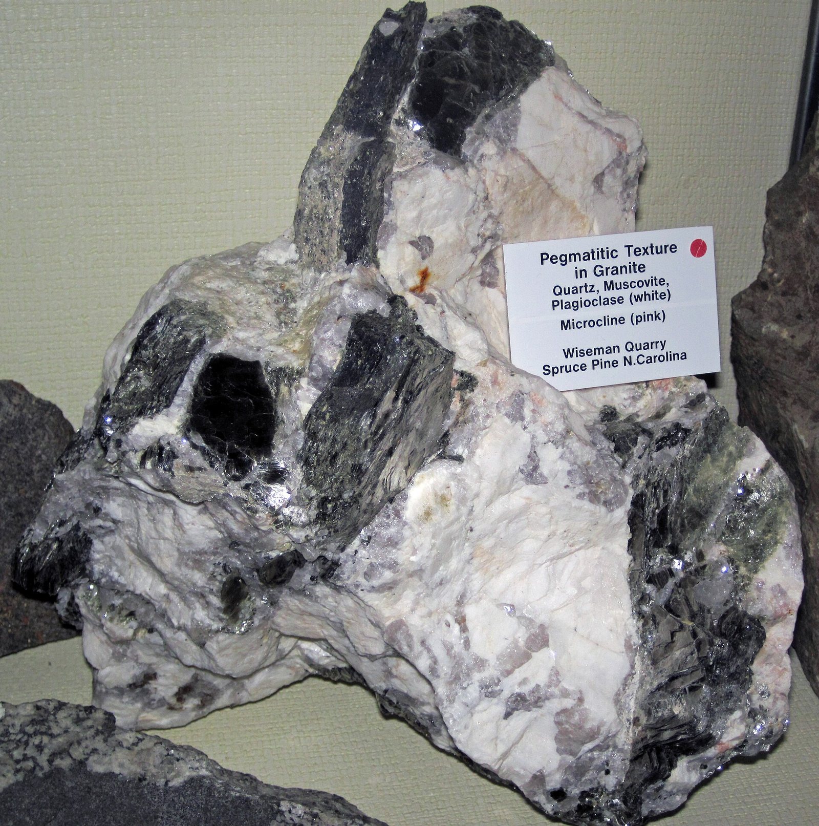
वास्तव में क्या चल रहा है
A silicon crystal is grown in a crucible of fused quartz, and any impurity in that crucible ends up in the chip. Only a few deposits on the planet are clean enough. The sand is not the product — it is the container the product is grown in, and it is consumed every time.
- सामग्री
- High-Purity Quartz
- प्रकार
- High-purity quartz sand, impurities measured in parts per million
- यह कहाँ से शुरू होती है
- United States — Spruce Pine, North Carolina — the source of most of the world's crucible-grade quartz
चरण दर चरण, और सीमा दर सीमा
United States · Spruce Pine, North Carolina द्वारा धारित Quartz producers (खनिक)
An unremarkable-looking quarry
Pegmatite is mined and the quartz separated from feldspar and mica. It then goes through a long purification sequence — flotation, acid leaching, chlorination — to strip aluminium, iron, titanium and sodium down to parts per million.
यहाँ क्यों: An accident of geology. These pegmatites formed with unusually little of the trace elements that ruin quartz for this purpose.
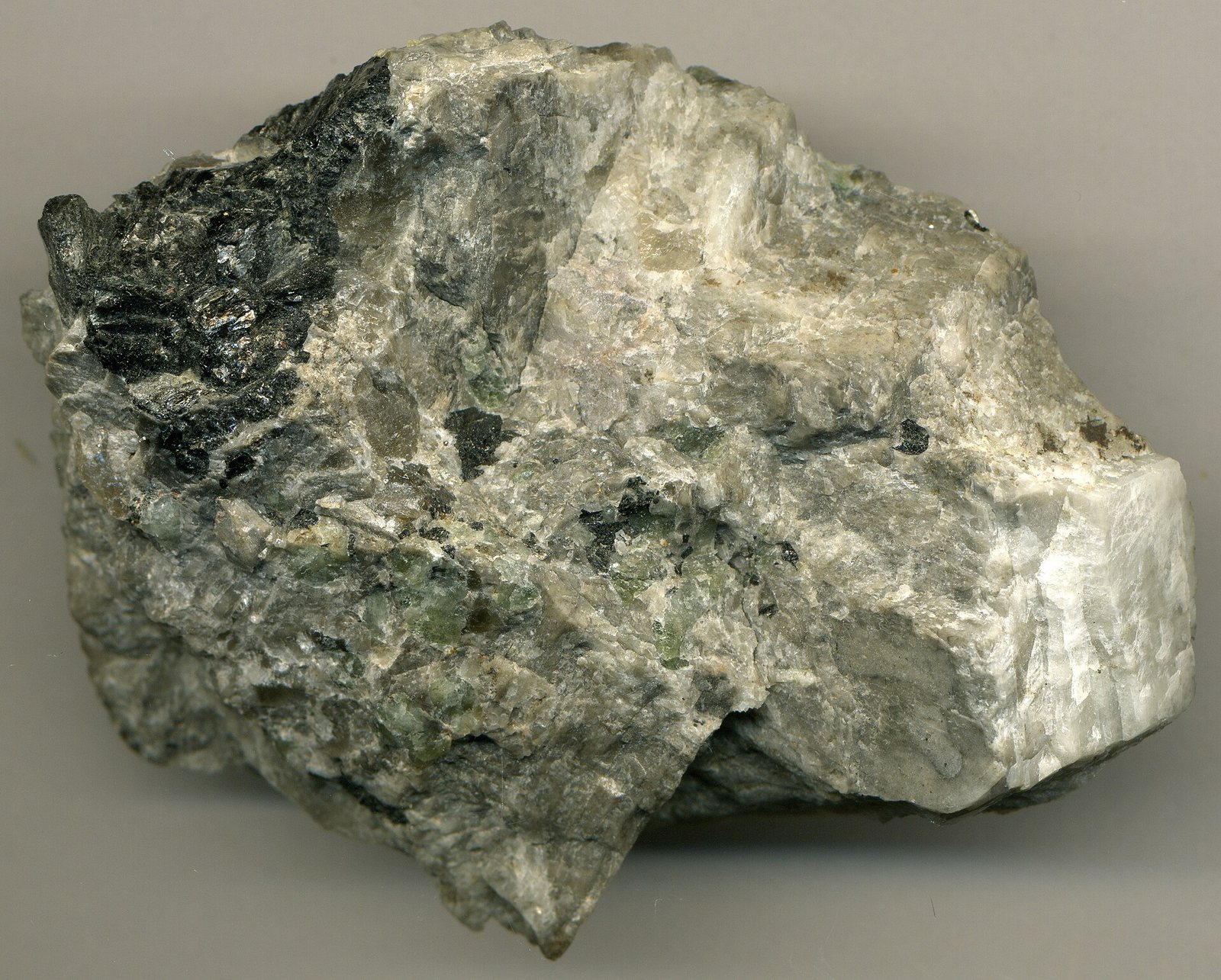
Germany · Fused-quartz manufacturers द्वारा धारित Crucible makers (निर्माता)
Made into crucibles
The sand is fused into crucibles — bowls that will hold molten silicon while a crystal is pulled from it.
यहाँ क्यों: Fused-quartz manufacture is its own specialised industry, separate from both mining and chipmaking.
China · Polysilicon plant द्वारा धारित Polysilicon producers (रासायनिक)
Meanwhile, the silicon itself
Ordinary quartzite is reduced with carbon to metallurgical silicon at about 99%, then converted to trichlorosilane, distilled and redeposited as polysilicon — up to eleven nines of purity for semiconductors.
शेष का क्या हुआ: This step is essentially electricity turned into purity, which is why it migrated to wherever power is cheapest.
यहाँ क्यों: Solar-grade polysilicon needs six or seven nines; semiconductor-grade needs eleven. The extra nines are what separate the two industries.
Japan · Crystal growers द्वारा धारित Wafer manufacturers (निर्माता)
Growing the crystal
Polysilicon is melted in the quartz crucible and a seed crystal is slowly pulled and rotated out of it, growing a single cylindrical crystal up to 300 mm across and two metres long.
शेष का क्या हुआ: The crucible is consumed. That is the whole reason this journey starts at a sand quarry rather than a silicon plant.
यहाँ क्यों: Crystal growing is dominated by a small number of Japanese, Korean, German and Taiwanese firms.
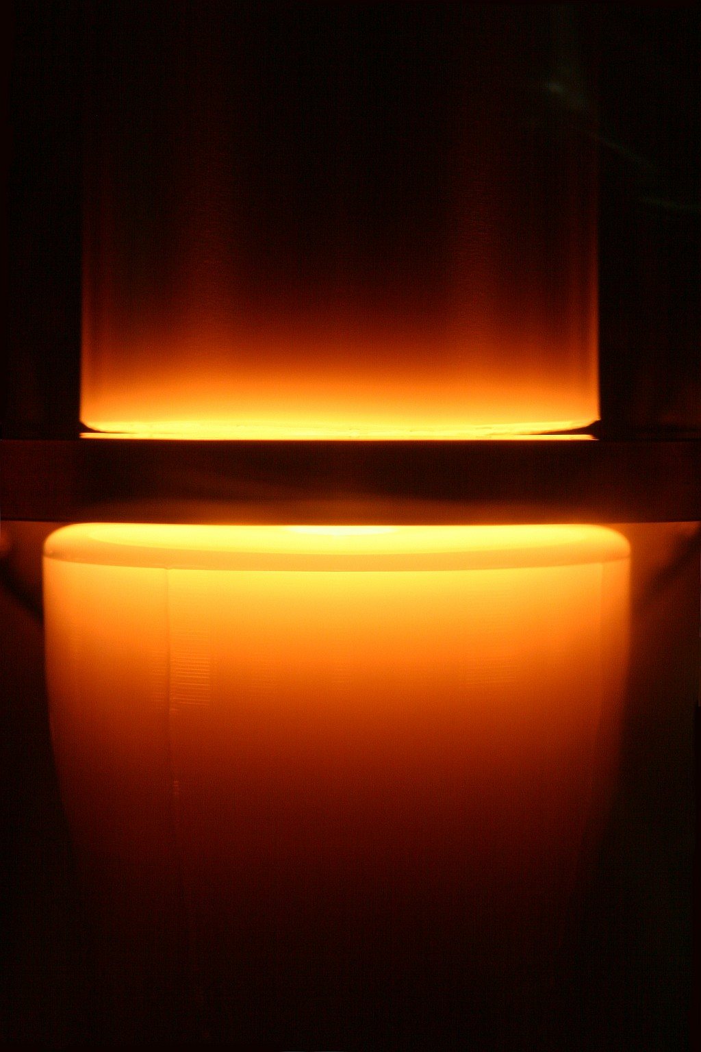
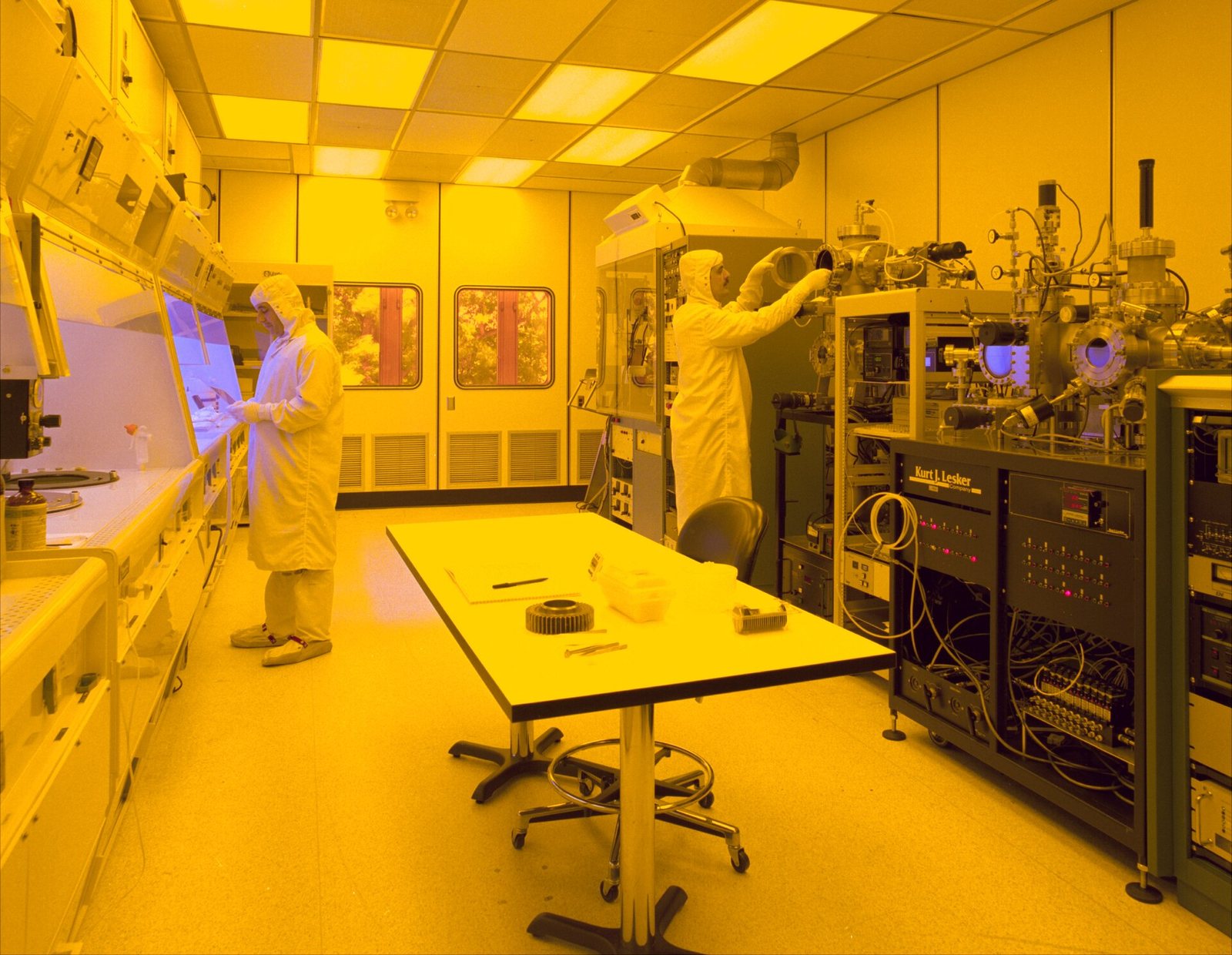
Taiwan · Fab, Hsinchu or Tainan द्वारा धारित Foundry (निर्माता)
Hundreds of steps on a wafer
Deposition, lithography, etch, repeated hundreds of times, building transistors and copper wiring layer by layer. Tungsten fills the contacts; hafnium oxide forms the gate dielectric; neon lases the light that prints the pattern.
यहाँ क्यों: Leading-edge fabs are among the most capital-intensive facilities ever built and exist in very few places.
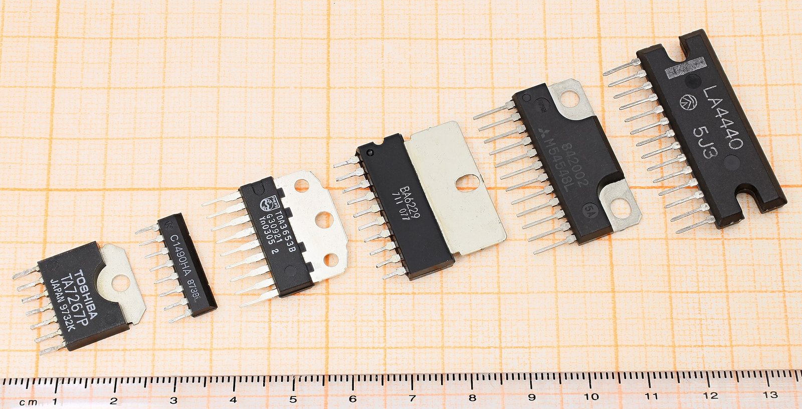
Vietnam · Assembly and test, then the world द्वारा धारित Assemblers and device makers (निर्माता)
Millions of chips
Wafers are diced, packaged, tested and soldered onto boards. From 1,000 kg of a specific sand from one American county, a few million finished chips.
यहाँ क्यों: Six countries and roughly six months, for something that weighs a few grams.
यह एक कार्यसाधित उदाहरण है। यह एक घोषित आरंभिक मात्रा को प्रकाशित सामान्य उपज और पुनःप्राप्ति दरों के माध्यम से अनुसरण करता है, इसलिए अनुपात जाँचे जा सकते हैं; यह किसी विशिष्ट शिपमेंट का अभिलेख नहीं है। मार्ग संबंधी तथ्य — कौन-से देश, कौन-सी प्रक्रियाएँ, और क्यों सामग्री को कहीं और संभाला नहीं जा सकता — सार्वजनिक रिपोर्टिंग से संकलित हैं।