鉱石から製品まで、経路を追跡
The Materials Atlas
素材 鉱山・鉱床 処理・精製 管理移転経路 サプライチェーン 企業 ニュース
棚別素材 バッテリー材料 希土類元素 銅・電気 半導体材料 核物質 航空宇宙・防衛 貴金属 鉄鋼・合金金属 工業用鉱物 農業用鉱物 エネルギー原材料 鉱石鉱物 周期表
需要 最終市場 技術 素材計算機 地図 スクリーナー
学習・ツール 学ぶ用語集 データに質問するAIエージェント 調査・データAPI ★ 保存済み
概要 運営について方法論 データソースお問い合わせ 免責事項
表示オプション
🧭 ガイドビュー 鉱石品位、精鉱、精錬、副産物といった用語が初めての方へ。閲覧しながらすべての用語をわかりやすく解説します。同じデータを、解説付きでご覧いただけます。
⚡ 専門家向け解説 業界の知識はお持ちのはず。データのみを——簡潔、迅速、コンパクトに、余分な説明なしで。これがデフォルト表示です。
テーマ
インターフェース言語
深度 素材ページは4段階のレベルで構成されている。任意の素材ページでレベルを選択すると、その設定が記憶される。
★ 保存済み 調査・データ
A quarry in North Carolina to the chip in your phone

管理移転経路 · 起点 United States

A quarry in North Carolina to the chip in your phone

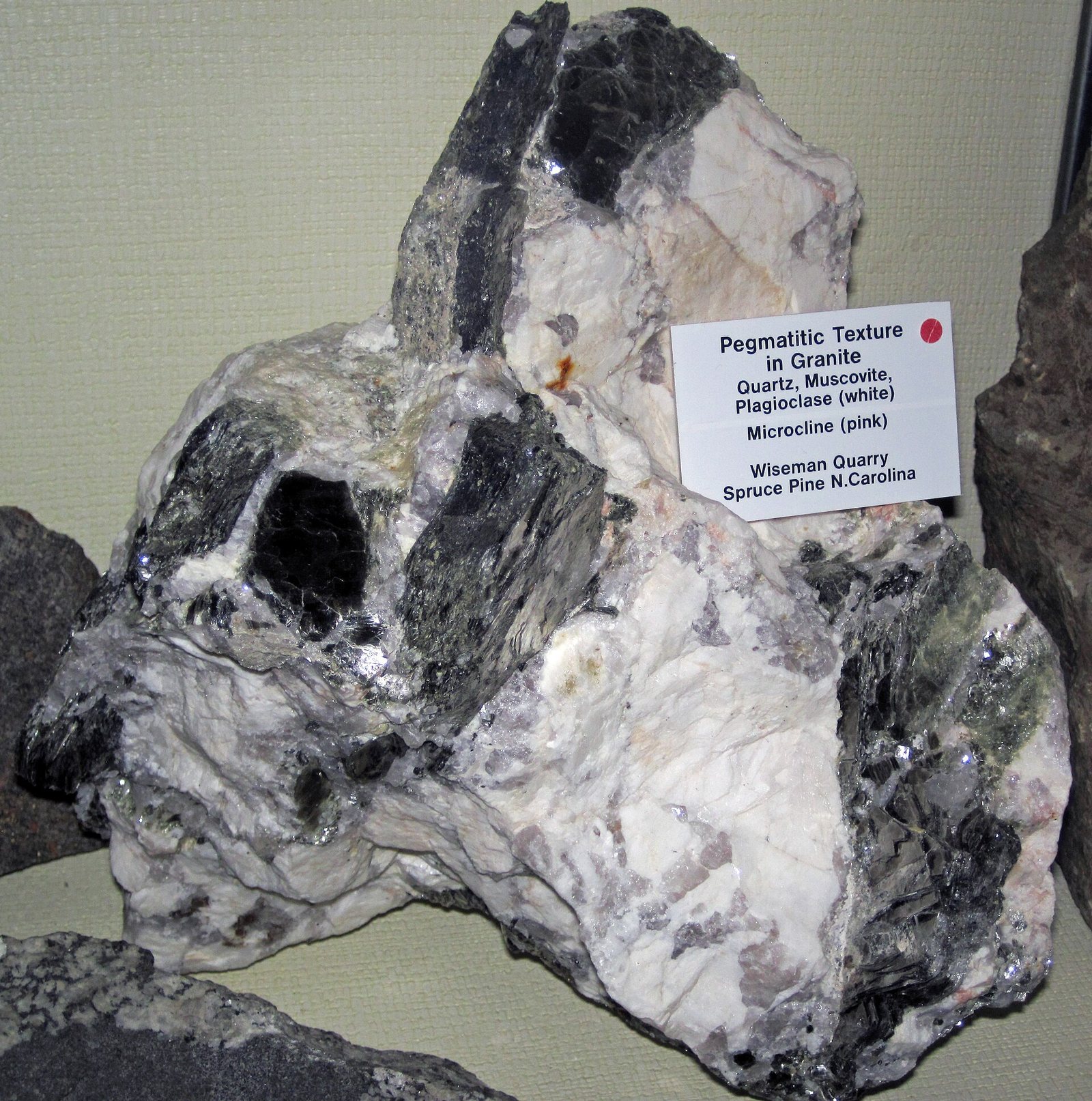
The most valuable sand on Earth, and almost all of it comes from one small district.

Pegmatitic granite (Spruce Pine Pegmatite District, Devonia… · James St. John · CC BY 2.0 · Wikimedia Commons
1,000 kg of high-purity quartz sand
8,000 wafers of 300 mm silicon, roughly
United States → Germany · Container Germany → China China → Japan Japan → Taiwan · Air freight Taiwan → Vietnam United States — An unremarkable-looking quarry 1 United States Germany — Made into crucibles 2 Germany China — Meanwhile, the silicon itself 3 China Japan — Growing the crystal 4 Japan Taiwan — Hundreds of steps on a wafer 5 Taiwan Vietnam — Millions of chips 6 Vietnam
素材の移動順に番号を付けた。国をクリックするとそのページが開く。 各国の重心から作成した正距円筒図法——弧は越境地点を示すものであり、実際の航路を示すものではない。

実際に動いているもの

A silicon crystal is grown in a crucible of fused quartz, and any impurity in that crucible ends up in the chip. Only a few deposits on the planet are clean enough. The sand is not the product — it is the container the product is grown in, and it is consumed every time.

素材
High-Purity Quartz
種類
High-purity quartz sand, impurities measured in parts per million
起点
United States — Spruce Pine, North Carolina — the source of most of the world's crucible-grade quartz
なぜこの経路で、別の経路ではないのか。 The crucible touches molten silicon at 1,400 °C for days. At that temperature it slowly dissolves, so every atom of contamination in it migrates into the crystal. That is why crucible quartz is specified to parts per billion and why so few deposits qualify.
最も細い連結点。 A handful of quarries, and one district in particular. It is the most cited single-point-of-failure in the semiconductor supply chain.
各工程の二つの数値を読む。投入量と産出量だ。数値が減少していく様子を追うことが要点である。最終的に、実際に機能する物質の数キログラムにまで、岩石1,000トンがどのように変化するかをたどることになる。

工程ごと、越境地点ごとに

01 採掘 1,000kg

United States · Spruce Pine, North Carolina 保管者 Quartz producers (採掘会社)

An unremarkable-looking quarry

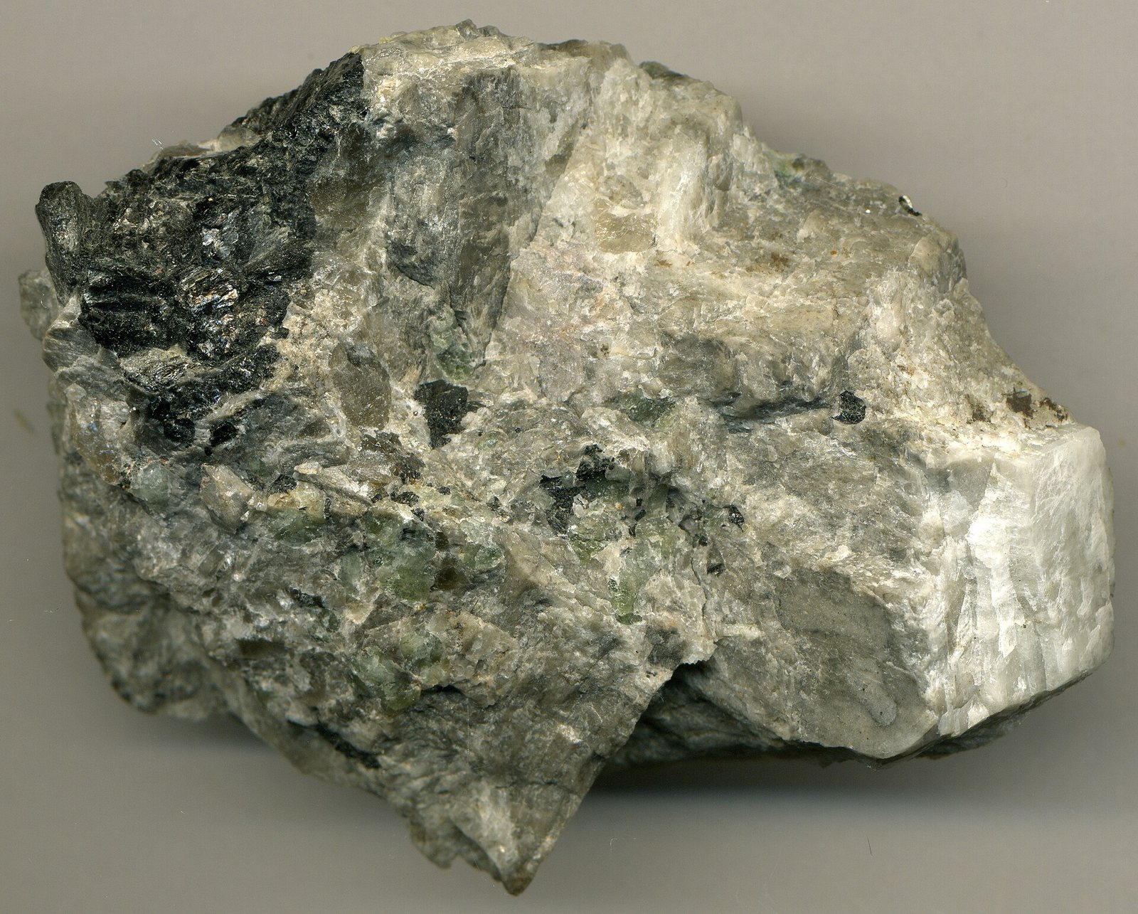
Pegmatite is mined and the quartz separated from feldspar and mica. It then goes through a long purification sequence — flotation, acid leaching, chlorination — to strip aluminium, iron, titanium and sodium down to parts per million.

1,000 kgquartz sand 1,000 kggraded high-purity sand

なぜここか: An accident of geology. These pegmatites formed with unusually little of the trace elements that ruin quartz for this purpose.
weeks Quartz →
An unremarkable-looking quarry
Pegmatitic granite (Tamminen Pegmatite,… · CC BY 2.0 via Wikimedia Commons
02 コンポーネント 1,000kg

Germany · Fused-quartz manufacturers 保管者 Crucible makers (製造業者)

Made into crucibles

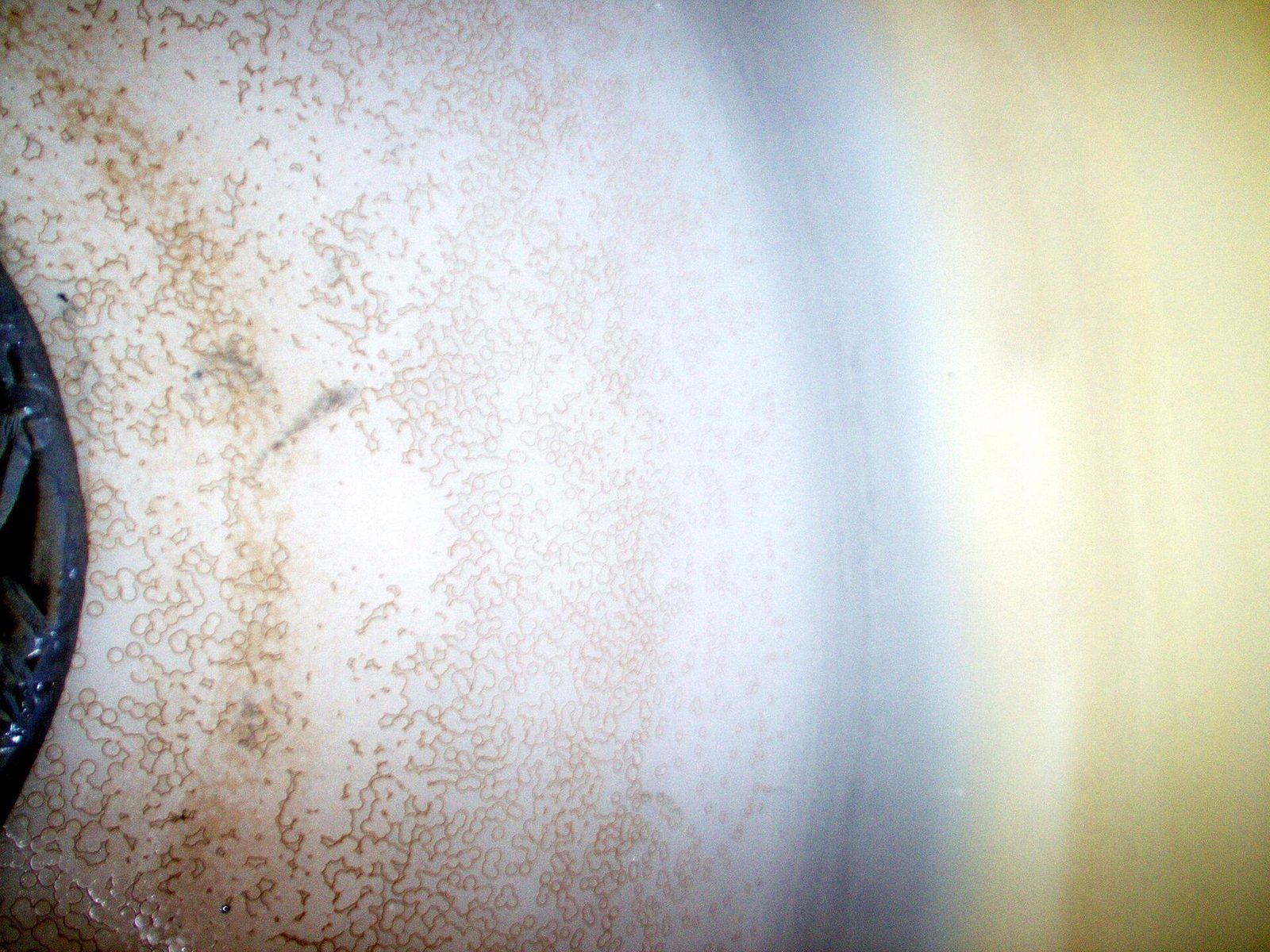
The sand is fused into crucibles — bowls that will hold molten silicon while a crystal is pulled from it.

1,000 kgsand 1,000 kgcrucibles

なぜここか: Fused-quartz manufacture is its own specialised industry, separate from both mining and chipmaking.
Container weeks High-Purity Quartz →
Made into crucibles
Czochralski method used crucible wall 2… · Public domain via Wikimedia Commons
03 処理

China · Polysilicon plant 保管者 Polysilicon producers (化学)

Meanwhile, the silicon itself

Ordinary quartzite is reduced with carbon to metallurgical silicon at about 99%, then converted to trichlorosilane, distilled and redeposited as polysilicon — up to eleven nines of purity for semiconductors.

残りはどうなったか: This step is essentially electricity turned into purity, which is why it migrated to wherever power is cheapest.

なぜここか: Solar-grade polysilicon needs six or seven nines; semiconductor-grade needs eleven. The extra nines are what separate the two industries.
選ばれなかった経路 Another chain with a single hard step Both are limited by one process almost nobody can do.
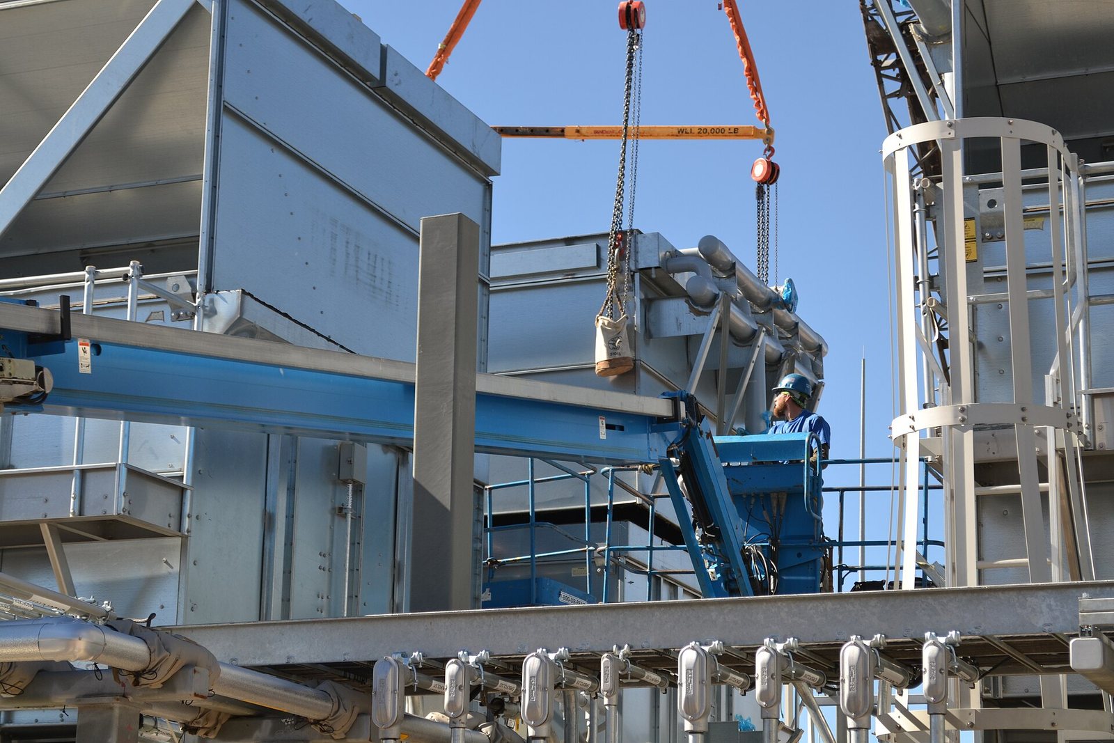
Hemlock Semiconductor Polysilicon Plant
Pueblo Chemical Agent-Destruction Pilot… · CC BY 2.0 via Wikimedia Commons
04 コンポーネント 8,000wafers

Japan · Crystal growers 保管者 Wafer manufacturers (製造業者)

Growing the crystal

Polysilicon is melted in the quartz crucible and a seed crystal is slowly pulled and rotated out of it, growing a single cylindrical crystal up to 300 mm across and two metres long.

1,000 kgcrucibles 8,000 wafers300 mm wafers this quartz can support

残りはどうなったか: The crucible is consumed. That is the whole reason this journey starts at a sand quarry rather than a silicon plant.

なぜここか: Crystal growing is dominated by a small number of Japanese, Korean, German and Taiwanese firms.
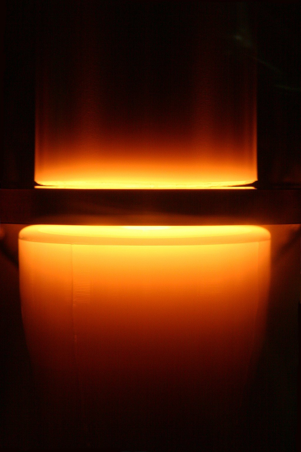
days per ingot Silicon →
Growing the crystal
Si-crystal floatingzone growing · CC BY-SA 3.0 via Wikimedia Commons
05 コンポーネント 8,000wafers

Taiwan · Fab, Hsinchu or Tainan 保管者 Foundry (製造業者)

Hundreds of steps on a wafer

Deposition, lithography, etch, repeated hundreds of times, building transistors and copper wiring layer by layer. Tungsten fills the contacts; hafnium oxide forms the gate dielectric; neon lases the light that prints the pattern.

8,000 wafersblank wafers 8,000 waferspatterned wafers

なぜここか: Leading-edge fabs are among the most capital-intensive facilities ever built and exist in very few places.
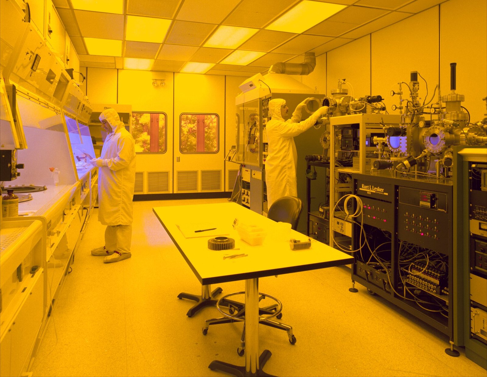
Air freight ~3 months per wafer TSMC Fab 18, Tainan →
Hundreds of steps on a wafer
Clean room · Public domain via Wikimedia Commons
06 最終市場 8,000wafers

Vietnam · Assembly and test, then the world 保管者 Assemblers and device makers (製造業者)

Millions of chips

Wafers are diced, packaged, tested and soldered onto boards. From 1,000 kg of a specific sand from one American county, a few million finished chips.

8,000 waferspatterned wafers 8,000 wafersdiced into millions of chips

なぜここか: Six countries and roughly six months, for something that weighs a few grams.
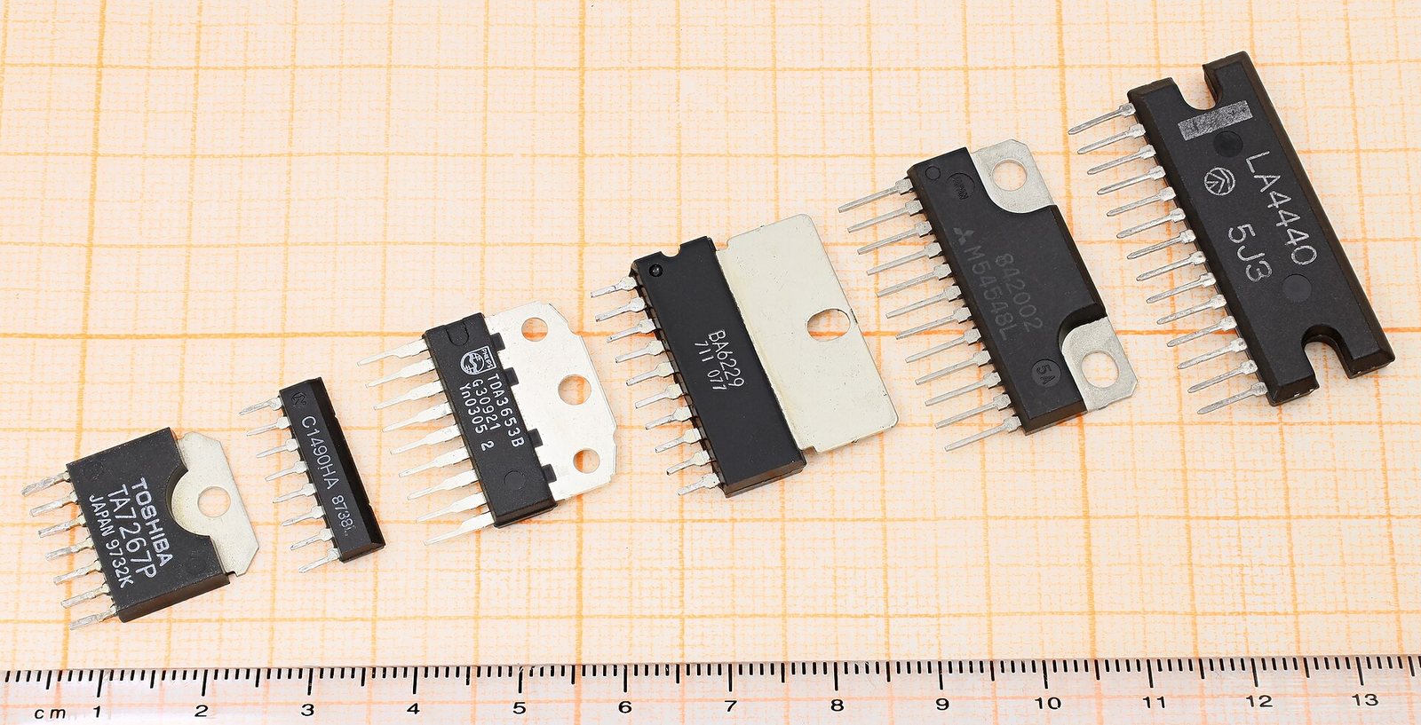
Millions of chips
SIP integrated circuits package · CC BY-SA 4.0 via Wikimedia Commons

これは計算例である。公表された標準的な歩留まりと回収率を用いて、明示された出発量を追うものであり、比率は検証可能だが、特定の荷物の記録ではない。経路に関する事実——どの国を経由するか、どのような工程を経るか、なぜその素材を他の場所では処理できないか——は公開情報から編集している。

素材

全素材 重要鉱物 レアアース バッテリー材料 鉱石鉱物 周期表 スクリーナー

地下

鉱山・鉱床 処理・精製 地図

経済

管理移転経路 サプライチェーン 最終市場 技術 企業 素材計算機

学ぶ

学ぶ用語集 データに質問するAIエージェント 調査・データオープンAPI ニュース★ 保存済み

運営について

運営についてお問い合わせ 方法論データソース 編集方針 プライバシーポリシー利用規約 免責事項