암석에서 제품까지, 추적
The Materials Atlas
소재 광산 및 광상 가공 및 정제 인수인계 여정들 공급망 기업 국가 뉴스
분류별 소재 배터리 소재 희토류 원소 구리 및 전기 반도체 소재 핵 물질 항공우주 및 방위 귀금속 철강 및 합금 금속 산업용 광물 농업용 광물 에너지 원자재 광석 광물 주기율표
수요 최종 시장 기술 소재 계산기 지도 스크리너
학습 및 도구 학습용어집 데이터에 묻기AI 에이전트 조사 및 데이터API ★ 저장됨
소개 소개방법론 데이터 출처문의 면책 조항
읽기 옵션
🧭 안내 보기 광석 품위, 정광, 정제, 부산물 등의 용어가 생소하신가요? 탐색하는 동안 모든 용어를 쉬운 말로 설명해드립니다. 동일한 데이터에 도움말이 내장되어 있습니다.
⚡ 전문가 보기 업계 사정에 익숙한 이용자를 위한 뷰. 데이터만, 군더더기 없이, 빠르고 간결하게, 추가 설명 없이 제공된다. 기본 보기로 설정되어 있다.
테마
인터페이스 언어
심도 소재 페이지는 네 가지 수준으로 작성되어 있습니다. 소재 페이지에서 수준을 선택하면 해당 설정이 기억됩니다.
★ 저장됨 조사 및 데이터
A quarry in North Carolina to the chip in your phone

인수인계 여정 · 시작 위치 United States

A quarry in North Carolina to the chip in your phone

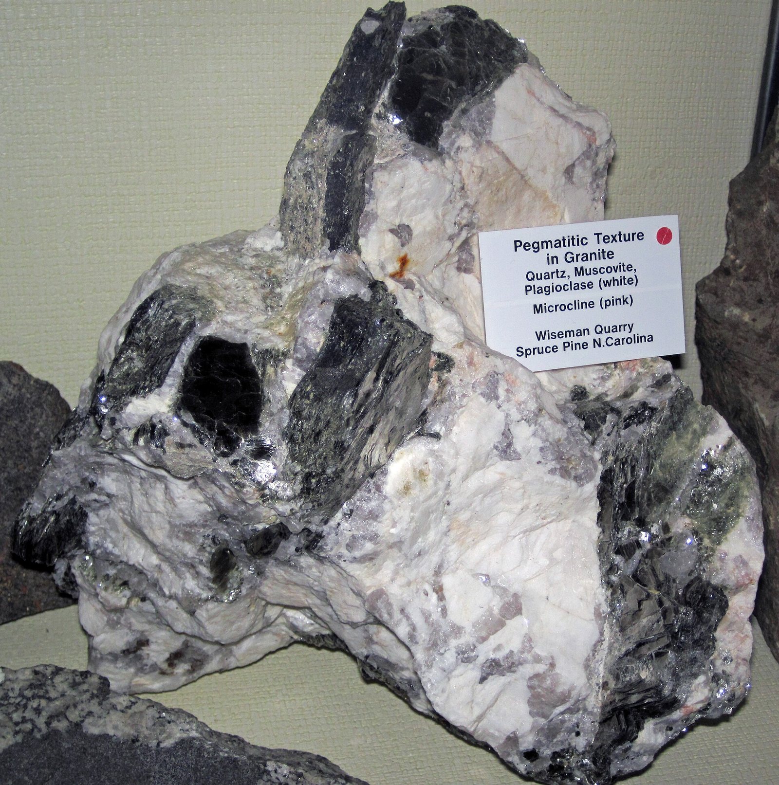
The most valuable sand on Earth, and almost all of it comes from one small district.

Pegmatitic granite (Spruce Pine Pegmatite District, Devonia… · James St. John · CC BY 2.0 · Wikimedia Commons
1,000 kg of high-purity quartz sand
8,000 wafers of 300 mm silicon, roughly
United States → Germany · Container Germany → China China → Japan Japan → Taiwan · Air freight Taiwan → Vietnam United States — An unremarkable-looking quarry 1 United States Germany — Made into crucibles 2 Germany China — Meanwhile, the silicon itself 3 China Japan — Growing the crystal 4 Japan Taiwan — Hundreds of steps on a wafer 5 Taiwan Vietnam — Millions of chips 6 Vietnam
소재가 이동하는 순서대로 번호가 매겨진다. 국가를 클릭하면 해당 페이지가 열린다. 국가 중심점을 기준으로 작성한 정거리원통 도법 — 호는 실제 항로가 아니라 통과하는 국경을 나타낸다.

실제로 이동하는 것

A silicon crystal is grown in a crucible of fused quartz, and any impurity in that crucible ends up in the chip. Only a few deposits on the planet are clean enough. The sand is not the product — it is the container the product is grown in, and it is consumed every time.

소재
High-Purity Quartz
유형
High-purity quartz sand, impurities measured in parts per million
출발지
United States — Spruce Pine, North Carolina — the source of most of the world's crucible-grade quartz
왜 이 경로인가, 다른 경로가 아닌 이유. The crucible touches molten silicon at 1,400 °C for days. At that temperature it slowly dissolves, so every atom of contamination in it migrates into the crystal. That is why crucible quartz is specified to parts per billion and why so few deposits qualify.
가장 좁은 연결 고리. A handful of quarries, and one district in particular. It is the most cited single-point-of-failure in the semiconductor supply chain.
각 단계에 표시된 두 수치를 읽어라. 투입량과 산출량이다. 수치가 줄어드는 과정을 지켜보는 것이 핵심이다. 마지막에 이르면 수천 톤의 암석이 실제로 쓰이는 물질 수 킬로그램으로 줄어드는 과정을 따라온 셈이 된다.

단계별, 국경별

01 채굴 1,000kg

United States · Spruce Pine, North Carolina 보유자 Quartz producers (채굴업체)

An unremarkable-looking quarry

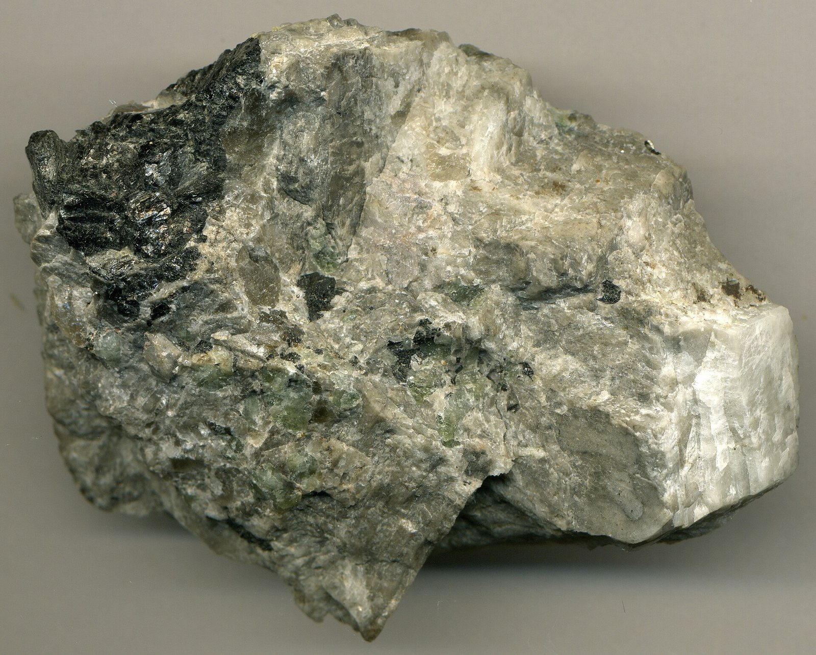
Pegmatite is mined and the quartz separated from feldspar and mica. It then goes through a long purification sequence — flotation, acid leaching, chlorination — to strip aluminium, iron, titanium and sodium down to parts per million.

1,000 kgquartz sand 1,000 kggraded high-purity sand

왜 이곳인가: An accident of geology. These pegmatites formed with unusually little of the trace elements that ruin quartz for this purpose.
weeks Quartz →
An unremarkable-looking quarry
Pegmatitic granite (Tamminen Pegmatite,… · CC BY 2.0 via Wikimedia Commons
02 구성 요소 1,000kg

Germany · Fused-quartz manufacturers 보유자 Crucible makers (제조사)

Made into crucibles

The sand is fused into crucibles — bowls that will hold molten silicon while a crystal is pulled from it.

1,000 kgsand 1,000 kgcrucibles

왜 이곳인가: Fused-quartz manufacture is its own specialised industry, separate from both mining and chipmaking.
Container weeks High-Purity Quartz →
Made into crucibles
Czochralski method used crucible wall 2… · Public domain via Wikimedia Commons
03 가공

China · Polysilicon plant 보유자 Polysilicon producers (화학)

Meanwhile, the silicon itself

Ordinary quartzite is reduced with carbon to metallurgical silicon at about 99%, then converted to trichlorosilane, distilled and redeposited as polysilicon — up to eleven nines of purity for semiconductors.

나머지는 어떻게 되었는가: This step is essentially electricity turned into purity, which is why it migrated to wherever power is cheapest.

왜 이곳인가: Solar-grade polysilicon needs six or seven nines; semiconductor-grade needs eleven. The extra nines are what separate the two industries.
선택하지 않은 경로 Another chain with a single hard step Both are limited by one process almost nobody can do.
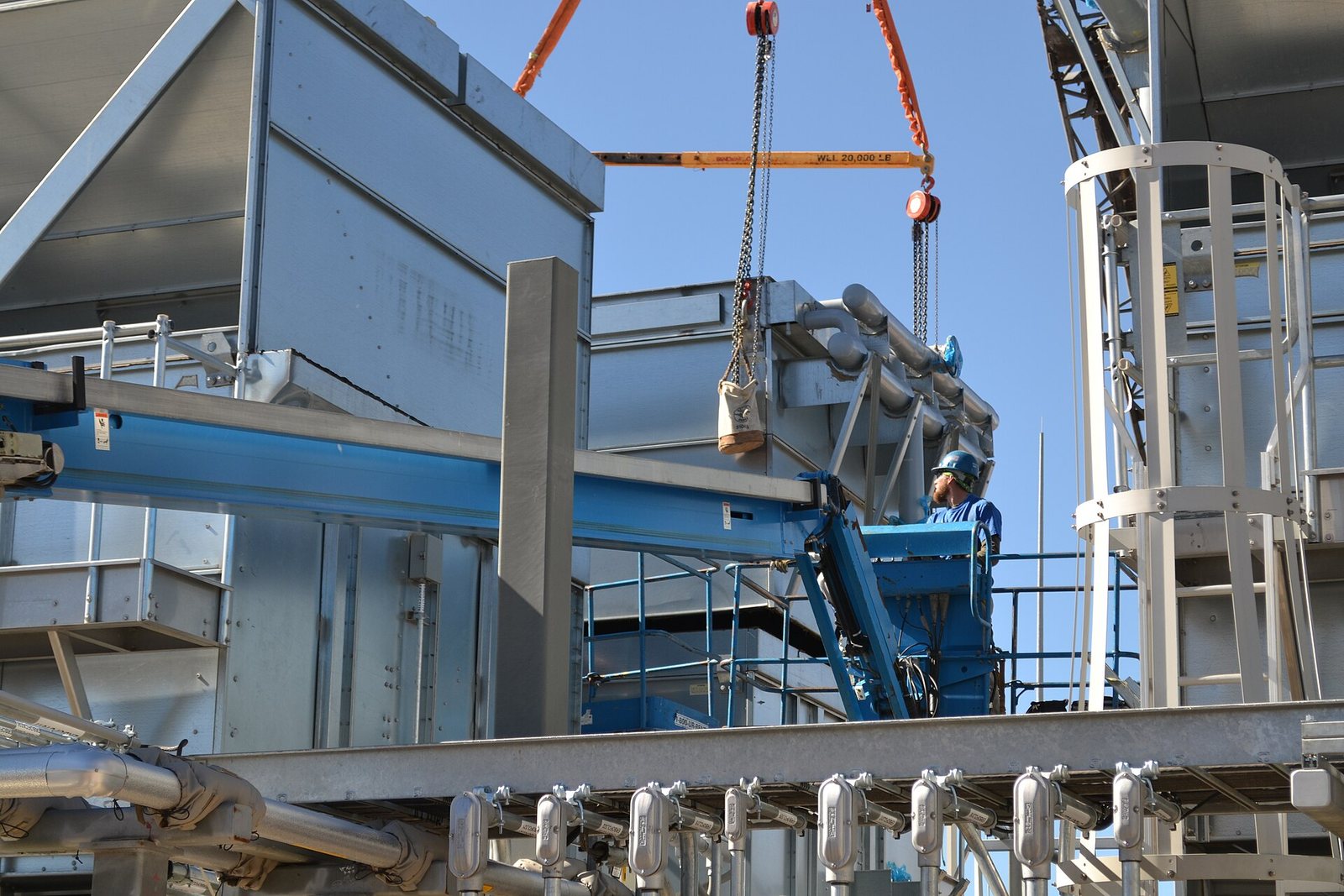
Hemlock Semiconductor Polysilicon Plant
Pueblo Chemical Agent-Destruction Pilot… · CC BY 2.0 via Wikimedia Commons
04 구성 요소 8,000wafers

Japan · Crystal growers 보유자 Wafer manufacturers (제조사)

Growing the crystal

Polysilicon is melted in the quartz crucible and a seed crystal is slowly pulled and rotated out of it, growing a single cylindrical crystal up to 300 mm across and two metres long.

1,000 kgcrucibles 8,000 wafers300 mm wafers this quartz can support

나머지는 어떻게 되었는가: The crucible is consumed. That is the whole reason this journey starts at a sand quarry rather than a silicon plant.

왜 이곳인가: Crystal growing is dominated by a small number of Japanese, Korean, German and Taiwanese firms.
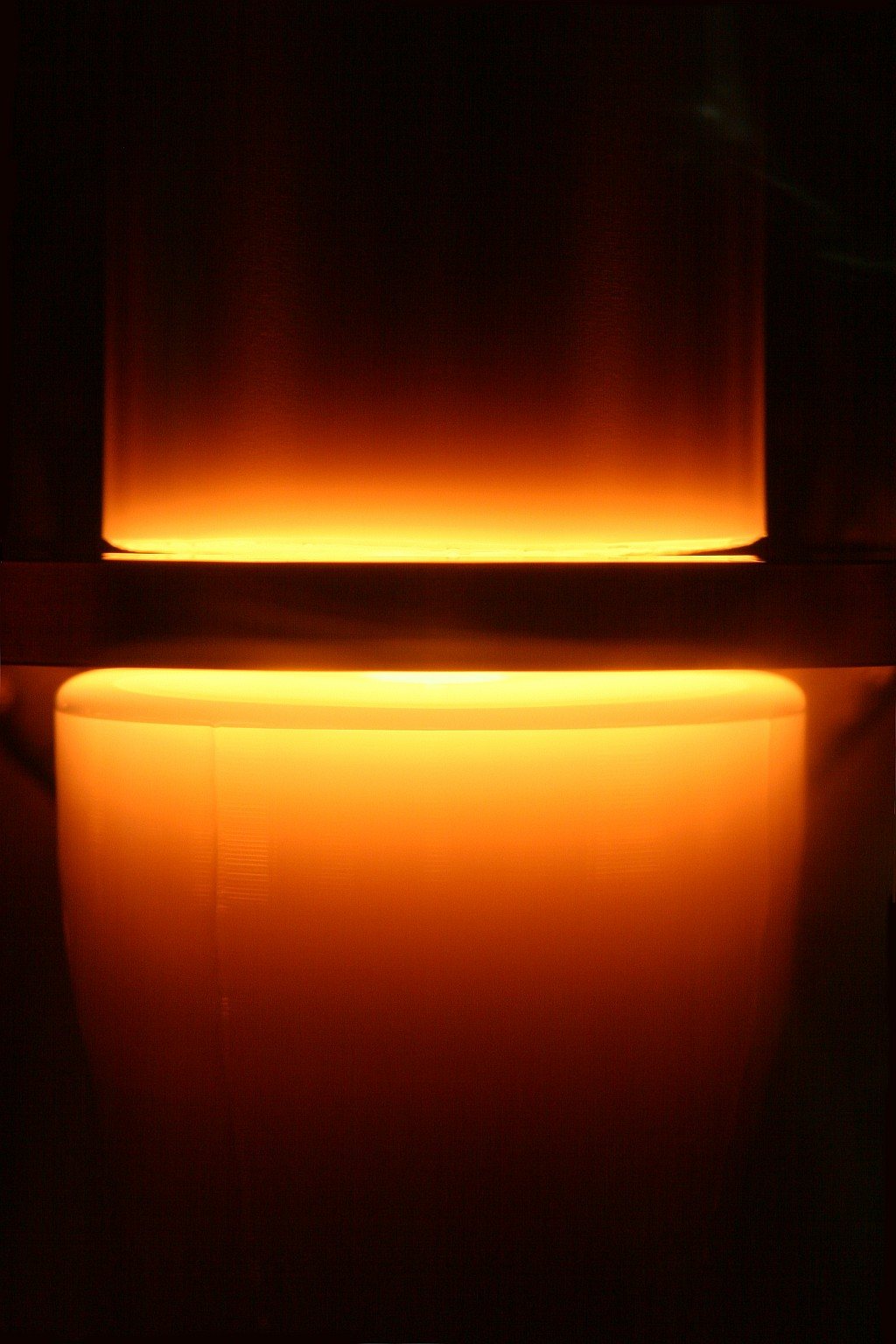
days per ingot Silicon →
Growing the crystal
Si-crystal floatingzone growing · CC BY-SA 3.0 via Wikimedia Commons
05 구성 요소 8,000wafers

Taiwan · Fab, Hsinchu or Tainan 보유자 Foundry (제조사)

Hundreds of steps on a wafer

Deposition, lithography, etch, repeated hundreds of times, building transistors and copper wiring layer by layer. Tungsten fills the contacts; hafnium oxide forms the gate dielectric; neon lases the light that prints the pattern.

8,000 wafersblank wafers 8,000 waferspatterned wafers

왜 이곳인가: Leading-edge fabs are among the most capital-intensive facilities ever built and exist in very few places.
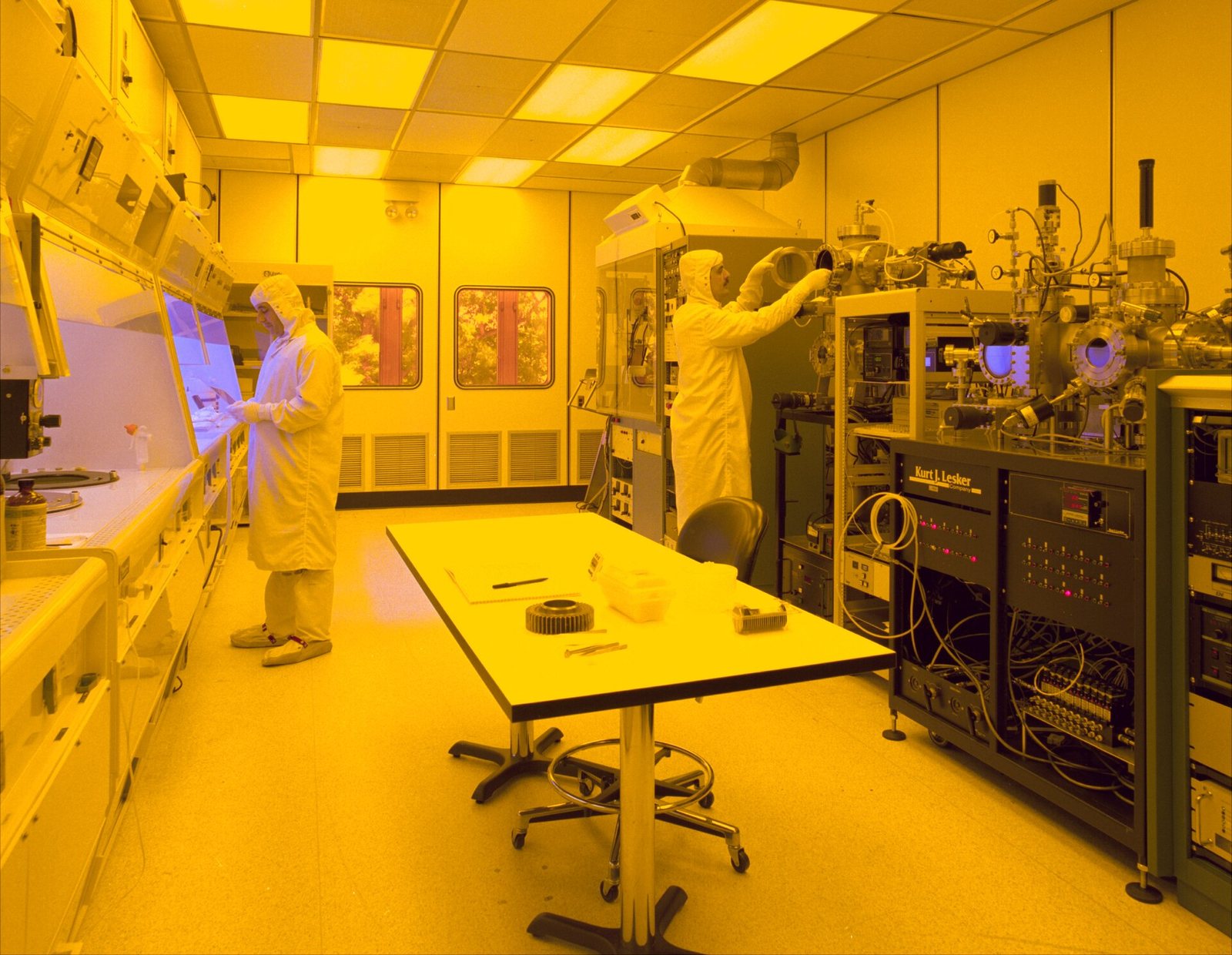
Air freight ~3 months per wafer TSMC Fab 18, Tainan →
Hundreds of steps on a wafer
Clean room · Public domain via Wikimedia Commons
06 최종 시장 8,000wafers

Vietnam · Assembly and test, then the world 보유자 Assemblers and device makers (제조사)

Millions of chips

Wafers are diced, packaged, tested and soldered onto boards. From 1,000 kg of a specific sand from one American county, a few million finished chips.

8,000 waferspatterned wafers 8,000 wafersdiced into millions of chips

왜 이곳인가: Six countries and roughly six months, for something that weighs a few grams.
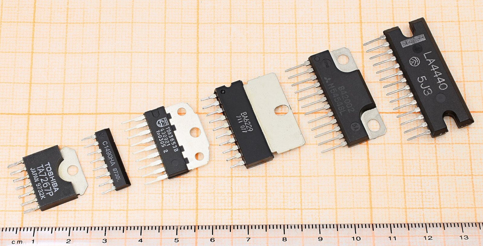
Millions of chips
SIP integrated circuits package · CC BY-SA 4.0 via Wikimedia Commons

이것은 작업 예시이다. 공표된 출발 수량을 공표된 일반적인 수율 및 회수율에 따라 추적한 것이므로 비율은 검증 가능하다. 특정 선적 기록이 아니다. 경로 사실—어느 나라, 어떤 공정, 그리고 왜 해당 소재를 다른 곳에서 처리할 수 없는지—은 공개 보고를 바탕으로 정리되었다.

소재

전체 소재 핵심 광물 희토류 배터리 소재 광석 광물 주기율표 스크리너

지하

광산 및 광상 가공 및 정제 국가 지도

경제

인수인계 여정들 공급망 최종 시장 기술 기업 소재 계산기

학습

학습용어집 데이터에 묻기AI 에이전트 조사 및 데이터공개 API 뉴스★ 저장됨

소개

소개문의 방법론데이터 출처 편집 방침 개인정보 처리방침이용 약관 면책 조항